


Optimizing PCB Internal Thermal Dissipation Through Advanced Thermal Modeling
Fast development of electronic technology leads to instant improvement in terms of computational speed, computational frequency and integrity of electronic products. Besides, with the volume of electronic products shrinking, volumetric power density is becoming increasingly high. In addition, the development orientation of thickness, lightness and miniature all make electronic components feature increasing calorific value of unit volume. With the upgrading of electronic products, their reliability is badly influenced as a result of fast increasing density of heat flow in PCBs. According to 10 degree principles, each time temperature rises by 10 Degrees Celsius, part of parameters of some components will decrease by a half. Based on a research, 55% of electronic devices are damaged because the temperature bypasses rated value of components. Therefore, reasonable component layout and PCB thermal dissipation has been the main elements engineers must consider.
Thermal design of electronic products is usually divided into the following levels: system level, board level and package level. Board level thermal design refers to the thermal design of radiator, electronic stencil and PCB. This article will provide a new method of dissipating heat that makes heat at the bottom of components fast transmitted to the outside and increases the thermal dissipation area of components without influencing PCB layout, which aims to reduce the temperature of components and temperature difference. Compared with traditional method of thermal dissipation, this new method has some attributes including multiple thermal dissipation structures, reduction of PCB thermal strain and small space occupation. The overall PCB thermal dissipation is anisotropic as a result of multiple patterns of PCB layers including top layer, bottom layer and routing layer that leads to the multiple features such as copper content, copper thickness, through holes and positions. Based on thermal analysis software and physical shape and thermal features of components, this article will set up simplified PCB and components and discuss the length, width and quantity of cooling fins with experiment results coming out through simulation data analysis of different conditions.
Thermal Analysis Principles
Thermal analysis theory at PCB board level is based on the basic principles of heat transfer theory. Heat transfer procedure features three different heat transfer modes: thermal conduction, thermal convection and thermal radiation, among which thermal conduction is the leading thermal dissipation method.
According to Fourier's law on heat transfer theory, at the differential layer with any thickness of d along the direction of x, energy passing d at unit time is directly proportional to the area A of temperature change rate, which can be displayed in formula 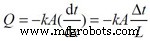 .
.
In this formula, Q (W) refers to the energy passing the area A at a unit time, which is also heat flow. A (m²) refers to the cross-sectional area at the conduction direction. L (m) refers to the length of conduction path. k [W/(m•°C)] is thermal conductivity. Δ t (°C) is the temperature difference between two sides of d. x (m) is the path of heat flow. Minus indicates the opposite to heat transmission direction and temperature increasing.
Density of heat flow q (W/m²) refers to the amount of heat flow passing through unit area A within unit time, which is shown in formula 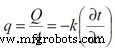 .
.
Different material has different thermal conductivity k whose high value indicates excellent conductivity.
PCB Thermal Resistance Theory
PCB is such a type of complicated multi-layer structure that its heat conduction is anisotropic. In terms of PCB thermal analysis, the material structure in each layer is different so that it's difficult to set up a model because of large grid numbers and slow computation speed. This article uses a simplified model with the help of thermal analysis software. The simplified multi-layer PCB model is displayed in Figure 1 below.
Suppose copper layer and FR-4 layer have the same thickness and each layer has the same spacing. kn that is normal thermal conductivity and kp that is thermal conductivity of each layer are used to describe thermal performance of PCB. The following formulas can be used to calculate the value of kn and kp.
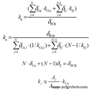
In this formula, δCu refers to the thickness of each copper layer; kCu is the thermal conductivity of copper with a value of 388[W/(m•°C)]; kj is the thermal conductivity of each copper routing; δF is the thickness of each FR-4 layer; kF is the thermal conductivity of FR-4 with a value of 0.35[W/(m•°C)]; δPCB is the overall PCB thickness; Aj is the overall area of copper routing on layer j. PCB thermal resistance is shown in the simplified model in Figure 2.
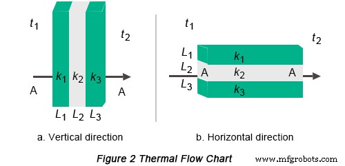
The temperature of PCB surface layer and bottom layer is respectively t1 and t2; the overall transmitted heat is Q; the overall resistance is R; the thermal resistance of each layer at thickness orientation is R1, R2 and R3 and at length L1, L2 and L3; the area of the board is A. Based on Figure 2(a), the orientation is supposed to be vertical only and thermal resistance can be calculated through the following formula:
R1 = L1(A•k1)
R2 = L2(A•k2)
R3 = L3(A•k3)
Based on Figure 2(b), the orientation is supposed to be horizontal only and thermal resistance can be calculated through the following formula:
R1 = L/(A1•k1)
R2 = L/(A2•k2)
R3 = L/(A3•k3)
1/R = 1/R1 + 1/R2 + 1/R3
The overall heat resistance along vertical and horizontal orientation can be displayed according to series-parallel connection of thermal resistance through formula Q = (t1 - t2)/R.
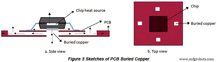
Based on the formula above, it is clear that overall thermal resistance on horizontal orientation is much lower than that on vertical orientation. Therefore, if copper is buried horizontally on PCB, better thermal dissipation effect will be obtained. A double-layer PCB is picked up by this article as an analysis object. Figure 3 is the sketch of PCB buried copper.
Simulation Analysis and Verification
• PCB Model Design
The size of simplified model is listed in below table.
| Item | Size |
| PCB | 100mm*100mm |
| Chip | 10mm*10mm |
| Component package | 20mm*20mm |
| Energy consumption of chip | 8W |
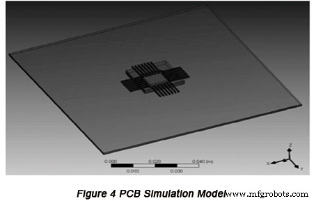
Component is placed at the center of PCB whose heat source has copper buried below. Copper cooling fins are buried adjacent to copper. Figure 4 is the simulation model with size of 0.5mmx30mm.
A circuit with 2A current is set as a simulation object so that line width is 0.5mm at least and through-hole 0.5mm. Cooling fins adjacent to buried copper should have min 1mm spacing and the width of cooling fins in this article are defined to be 0.13mm, 0.25mm, 0.5mm, 0.75mm and 1mm and length 20mm, 30mm and 40mm. Under the condition of 10mm width and less than 1mm spacing, the number of cooling fins with different width is displayed in below table.
| Fin width (mm) | Temperature (°C) | Fin length (mm) | Number of fins | ||
|---|---|---|---|---|---|
| 20 | 30 | 40 | |||
| 0.13 | Highest | 96.7 | 91.2 | 89.8 | 10 |
| Lowest | 89.1 | 84.5 | 83.4 | ||
| 0.25 | Highest | 92.5 | 89.5 | 87.5 | 8 |
| Lowest | 85.4 | 83.6 | 81.9 | ||
| 0.50 | Highest | 92.1 | 88.6 | 86.2 | 7 |
| Lowest | 85.3 | 83.2 | 81.2 | ||
| 0.75 | Highest | 91.9 | 87.9 | 85.3 | 6 |
| Lowest | 85.2 | 83.0 | 80.8 | ||
| 1.00 | Highest | 91.8 | 87.8 | 85.1 | 5 |
| Lowest | 85.0 | 82.9 | 80.8 | ||
| Temperature of components without buried copper (°C) |
Highest: 108.4 Lowest: 98.3 |
||||
• Result Analysis
Based on Table 2, it can be inferred that differences in terms of width and length of copper fins all lead to the great escalation of component temperature of PCBs. however, in the practical application, suitable PCB length and fin width should be picked up considering practical situations and cost of copper. Figure 5 is the graph of highest temperature of components while Figure 6 is the graph of lowest temperature of components.
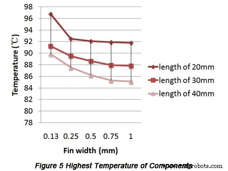
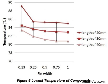
From the change tendency indicated by the graph, it can be summarized that when the width of fins is less than 0.5mm, the temperature of components is greatly decreased with the enlargement of fin width. Temperature reduction becomes steady when the width is more than 0.5mm. Thus, temperature difference is the largest when fin width is kept 0.5mm with the lowest material cost. With the increase of cooling fins, component temperature decreases.
Temperature falls at the largest extent, more than 5°C when fin length is in the range from 20mm to 30mm. Temperature falls at small extent, more or less than 2°C when fin length is in the range from 30mm to 40mm. Therefore, reducing temperature differences are relatively large when fins with length of 20mm to 30mm are picked up with the relatively low cost. Considering the fact that PCB cooling fins can neither be too long nor too wide, it's suitable to pick up fins whose width is 0.5mm and length 30mm.
Figure 7 is the graph of PCB simulation temperature distribution without buried copper while Figure 8 is the graph of PCB simulation temperature distribution with fins whose length is 30mm and width 0.5mm.
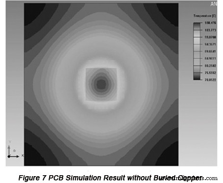
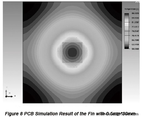
According to the two figures, it can be known that the highest temperature falls from 108.4°C to 88.6°C, with a reduction extent of 18.5%. The lowest temperature falls from 98.3°C to 83.2°C, with a reduction extent of 15.3%. Based on the comparison in terms of temperature field between Figure 7 and Figure 8, PCB with buried copper is capable of helping the temperature field distributed evenly and reducing the temperature difference of boards so that hot spots can be avoided. PCB with buried copper reduces the temperature of components, which is beneficial to the improvement of thermal dissipation of components on PCB so that reliability of components will be greatly increased.
Helpful Resources
• The Most Comprehensive Principles of Thermal Design for PCBs
• Tips of Thermal Design for PCBs Controlled by FPGA System
• Design of High-Power PCB in High Temperature Environment
• Metal Core PCB an Ideal Solution to Thermal Issues in PCB and PCBA
• Full Feature PCB Manufacturing Service from PCBCart - Multiple Value-added options
• Advanced PCB Assembly Service from PCBCart - Start from 1 piece
Industrial Technology
- Advanced Heat Dissipation Techniques for Reliable PCB Performance
- Optimizing Thermal Management: Advanced Heat Sink PCB Design
- Choosing the Right PCB Layout Software: Expert Comparison & Recommendations
- Create NC Drill Files for Your PCB Design Software: A Step‑by‑Step Guide
- Create Gerber Files from Any PCB Design Software – A Complete Guide
- From Schematic to PCB: A Comprehensive Altium Designer Workflow
- Mastering PCB Thermal Design: Essential Principles for Reliability
- Expert PCB Thermal Design: Practical Tips for Heat Management
- Designing High‑Power PCBs for High‑Temperature Environments
- Advanced PCIe High-Speed Password Card PCB Design - Research & Innovation