


6 Essential Steps to Master Solder Mask Design and Selection
Protecting your PCB from oxidation, corrosion, and solder‑bridge failures begins with the right solder mask. Below is a concise, industry‑backed guide that covers everything from fundamentals to manufacturing best practices.
What Is a Solder Mask?
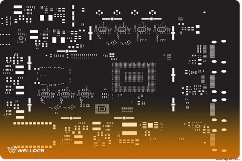
A solder mask—also known as solder resist or solder‑stop—is a thin, resin‑based coating that blankets the copper traces on a PCB. Its primary purpose is to prevent solder from bridging adjacent pads during reflow or hand soldering, while also shielding the copper from moisture, dust, and oxidation. The most common formulation is a thermosetting epoxy resin, chosen for its excellent insulation, humidity resistance, high‑temperature tolerance, and solder‑resistance properties.
While green remains the traditional color, manufacturers now offer a palette of options—white, black, blue, yellow, red, and more—to give boards a unique identity or to meet niche requirements (for example, red is popular in AI and black in high‑light‑reflection applications).
Custom color selections can also serve as a quick visual cue during assembly, helping teams identify boards from the same supplier or project line.
Key Functions of a Solder Mask
The solder mask is critical for:
- Preventing solder bridges and short circuits during reflow.
- Protecting copper traces from corrosion, oxidation, and contamination.
- Providing a clean, insulating surface for component placement.
Without it, hand‑assembled boards are prone to short circuits, and mass‑produced boards risk reliability issues. That’s why virtually every commercial PCB includes a solder mask.

Four Common Solder Mask Technologies
Each technology offers distinct advantages depending on cost, resolution, and production volume:
- Top and Bottom‑Side Masks – Applied via ink, epoxy, or film, these masks cover both sides of the board, allowing for selective openings where component pads are located.
- Epoxy Liquid – A cost‑effective, thermosetting polymer that can be screen‑printed and thermally cured. Ideal for small‑run or prototyping projects.
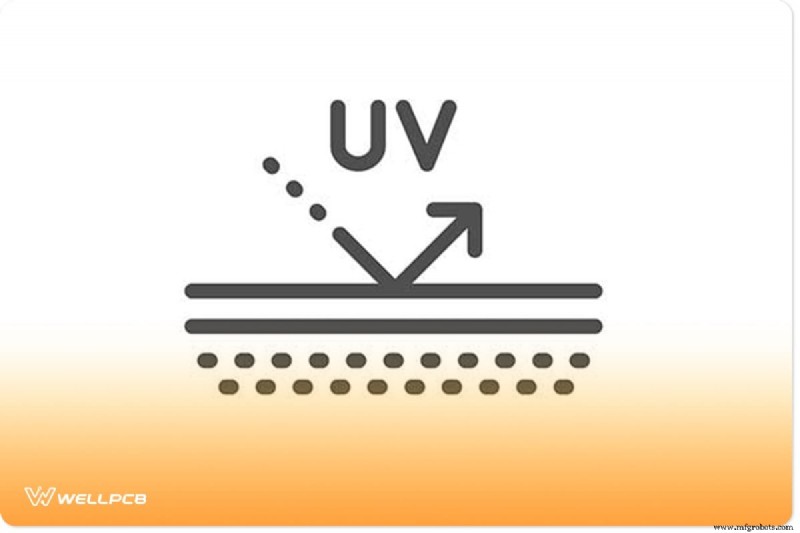
- Liquid Ink Photo‑Imageable – Spray‑applied ink that is exposed to UV light through a photomask and then developed. Offers high resolution for fine‑pitch designs but requires clean, controlled environments.
- Dry Film Photo‑Imageable – A laminated film that is exposed and developed, then removed. Provides excellent uniformity and is commonly used in high‑volume manufacturing.

Manufacturing Process Overview
The solder mask application workflow is meticulous to ensure consistency and reliability:
- Cleaning – Thoroughly remove flux, dust, and oils to create a pristine substrate.
- Ink Coating – Deposit a controlled thickness of mask ink via vertical coating or inkjet, depending on the chosen technology.
- Pre‑Hardening – Stabilize the ink before exposure to remove excess material during development.
- Imaging & Hardening – Align a transparent film or mask, expose to UV, and cure to lock the pattern in place.
- Developing – Submerge the board in a developer solution to wash away unexposed ink, revealing the copper pads.
- Final Hardening & Cleaning – Perform a final cure to achieve the desired mechanical properties, then clean the board for downstream processes.
Design Tips for a Reliable Solder Mask
Choosing the correct mask is only part of the equation. Your PCB design must be mask‑ready to avoid costly rework:
- Verify pad sizes and spacing in the design files to ensure adequate mask clearance.
- Avoid overly tight tolerances that could cause short‑circuiting during soldering.
- Use a reputable PCB manufacturer to confirm their capabilities and mask tolerances before finalizing the design.

Choosing the Right PCB Manufacturer
Partnering with a seasoned manufacturer is crucial for cost efficiency and quality assurance. Key factors to evaluate include:
- Specialization – Determine whether the vendor offers fabrication, assembly, or both.
- Quality Control – Request a demonstration of their inspection and testing protocols.
- Experience – Look for a track record in high‑volume or high‑complexity PCBs.
- Certifications – Verify compliance with industry standards such as IPC‑JSTD‑001, ISO 9001, or ISO 14001.
Conclusion
With a clear understanding of solder mask functions, types, and manufacturing steps, you can make informed decisions that enhance PCB reliability and reduce failure rates. Contact us to discuss your project’s specific requirements, explore our color and customization options, and take advantage of bulk‑order discounts.
Protect your investment and extend your PCB’s lifespan—let our expertise guide you from concept to final assembly.
Industrial Technology
- Resistor Types Explained: From Potentiometers to Thermistors
- Accurate Resistance Measurement: Digital vs. Analog Multimeter Guide
- Mastering Time Constant Calculations for RC and RL Circuits
- Mastering Thin-Walled CNC Turned Parts: Expert Tips for Strength & Precision
- Accelerate Design with 3D Printing Prototypes: Boost Efficiency & Accuracy
- Revolutionizing Industrial Visits: Virtual On‑Site Experiences Deliver Real‑World Value
- 4 Reasons the Cheapest Metal Fabrication Quote Can Backfire
- Expert PCB Thermal Design: Practical Tips for Heat Management
- Common Challenges in Transportation Design Engineering
- The Ultimate Guide to Choosing Asset Management Software