


Bare PCB Design & Manufacturing: Expert Steps for Engineers
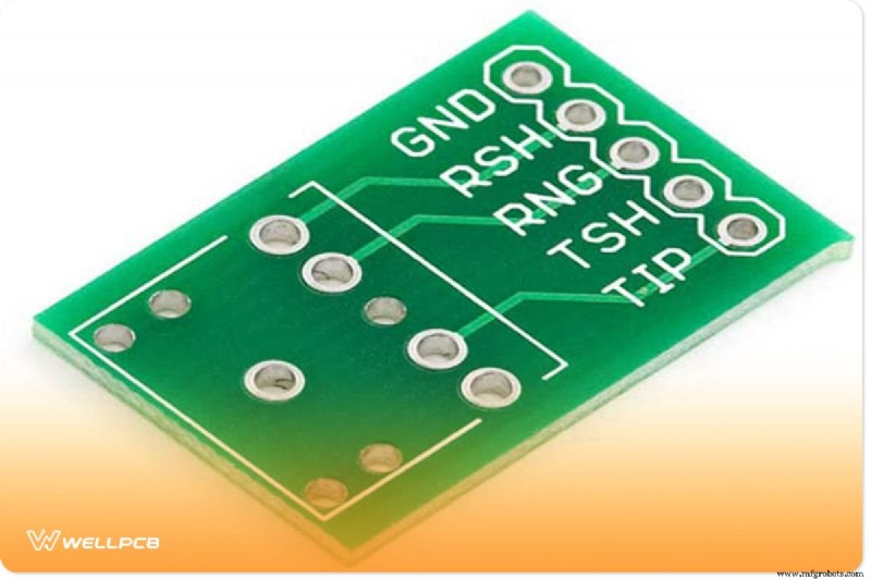
As the name implies, a bare PCB is the blank canvas that engineers tailor to host their specific components. Crafting a board that meets performance and reliability goals requires meticulous design, precise manufacturing, and rigorous inspection.
In modern electronics—from smart calculators to sophisticated digital clocks—printed circuit boards are the critical backbone that routes current across copper pathways on a substrate. Their role is to guide electrons exactly where they’re needed.
Designing a Bare PCB
Before you start drafting, consult with your PCB manufacturer. Early collaboration can prevent costly errors and ensures your design aligns with production capabilities.
Step 1: Design & Export
Your board must adhere to industry standards such as IPC‑2221. Use reputable EDA tools—KiCad, OrCAD, Altium Designer, or Eagle—to create a rigorous layout. Specify the software version for the manufacturer to avoid version‑related discrepancies.
Once the design is approved, export Gerber files (the industry‑standard format). Gerbers encode all essential information: copper layers, drill data, solder masks, silkscreen, and more. The files undergo a checksum check to catch errors before fabrication.
Critical parameters to define include trace width, spacing, via size, edge clearance, and drill tolerances—all of which influence signal integrity and manufacturability.

Step 2: Photo‑Mask Creation
The manufacturer converts your Gerbers into photomasks using high‑resolution plotters. These masks are negative images that define where copper is deposited or etched away.
Each layer—typically two for a standard PCB—requires its own mask. Aligning layers accurately is critical; misalignment can lead to open circuits or shorted traces.
Inspection & Testing
Visual inspection is adequate for two‑layer boards, but multi‑layer boards demand electrical testing to ensure trace integrity.
Common test methods include:
- Flying‑probe test – a portable probe that contacts test points without fixtures.
- Bed‑of‑nails (Universal Grid) test – uses a fixture that holds the board and probes all test points simultaneously.
Tests typically measure:
- Resistance – verifies continuity and checks for open traces; longer traces exhibit proportionally higher resistance.
- Capacitance – detects unintended coupling or shorts between adjacent traces.
For critical applications, additional diagnostics like In‑Circuit Test (ICT) or Automatic Test Equipment (ATE) can be employed to catch subtle defects.
Industrial Technology
- Unlock Operational Excellence with ATS Manufacturing Data Analytics
- AI Revolutionizes Factory Robots: Smarter, Safer, More Efficient
- Understanding Conductance, Susceptance, and Admittance in AC Circuits
- Electric Pendulum: How Capacitors and Inductors Exchange Energy
- Is Your Factory Ready for Smart Manufacturing? Unlock the Power of Industry 4.0
- Why IPC Standards Are Essential for Quality PCB Assembly
- Understanding Cobots: Collaborative Robots in Modern Industry
- Designing Optimal Bin Storage: Key Traits for Efficient Fabrication
- The Critical Role of Unique Identification in Industrial Asset Management
- Summer Spotlight: DVIRC Pets and Their Playful Manufacturing Careers