


Ultiboard: A Comprehensive Guide for Beginners
Electronic circuit design has evolved into a highly precise discipline where accuracy and speed are paramount. A well‑crafted PCB layout is the foundation for a reliable final product, and any shortcut can compromise performance or increase costs. This guide walks you through every step of working with Ultiboard – from downloading and installing the software to creating a circuit, navigating its interface, and exporting a manufacturing‑ready file.
What Is Ultiboard?
Ultiboard, originally known as ULTIboard, was developed by Ultimate Technology in the Netherlands. Historically priced between $800 and $2,500, the tool was accessible only to a select group of professionals, with a limited student version available on the market. Over time, it evolved into a powerful suite that now includes schematic capture, simulation, and PCB layout capabilities, often used in conjunction with National Instruments’ Multisim for a seamless design workflow.
Core Functions
- Intuitive PCB layout and routing tools that streamline design work.
- Advanced spreadsheet view, design wizards, and toolbox for efficient component placement.
- Seamless integration with Multisim™ for direct transfer of schematics to board layouts.
- Export options in industry‑standard formats such as Gerber and DXF for manufacturing.
Ultiboard is widely adopted by engineers, manufacturers, educators, and students alike for its flexibility, speed, and comprehensive feature set.
Downloading and Installing Ultiboard
Before installation, verify that your system meets the minimum requirements for Ultiboard 9: a 150 MB download, Windows 2000/XP, Pentium III processor, 128 MB RAM, CD-ROM, and an 800×600 screen resolution. Older hardware may struggle, so consider upgrading if you encounter performance issues.
The official National Instruments website hosts both professional and academic versions. Installation is straightforward—simply follow the on‑screen prompts. Once installed, spend some time exploring the interface to build familiarity before starting a new project.
User Interface Overview
Ultiboard’s layout is designed for rapid creation and fine‑tuned control. The main toolbar contains familiar icons—hover over any icon for a tooltip that explains its function. The design workspace is complemented by a spreadsheet view, design toolbox, and 3‑D viewer for detailed inspection.
Primary Toolbar Icons
- Select – Pick elements on the board.
- Design Toolbox – Toggle the toolbox visibility.
- Spreadsheet View – Show or hide the spreadsheet tab.
- Database Manager – Access the component database.
- Board Wizard – Launch the board outline wizard.
- Part Wizard – Add components via the wizard.
- Place from Database – Browse and place components.
- Line / Follow‑Me / Polygon / Power Plane – Draw traces and planes.
- DRC & Netlist Check – Run design rule checks.
- Text – Add labels or notes.
- View 3D – Open the 3‑D preview.
- Capture Screen – Screenshot a portion of the canvas.
- Help – Access the Ultiboard help system.
Edit Toolbar Functions
- In‑Place Part Edit – Modify components directly on the board.
- Swap Layer – Move elements to the mirrored layer.
- Rotate 90° CW/CCW – Rotate selected items.
Customizing Preferences
- Navigate to
Options > Global Preferencesto access tabs such as General, Paths, Colors, PCB Design, Dimensions, and 3‑D Options. - Adjust settings per your workflow.
- Click
OKto apply changes.
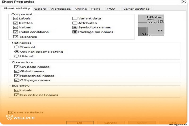
Setting PCB Properties
Right‑click on an empty board to open the Sheet Properties dialog, where you can define layer stack‑ups, board dimensions, and design rules.
Design Toolbox & Spreadsheet View
The Design Toolbox provides quick access to frequently used tools, while the Spreadsheet View displays attributes, footprints, and reference designators for each component.
Customizing the Interface
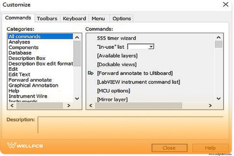
Use Options > Customize User Interface to rearrange toolbars, add or remove icons, and tailor the workspace to your preferences.
Getting Started with a Simple Design
The Electronics Workbench Suite
Ultiboard is part of the Electronics Workbench suite, which includes:
- Multisim – Integrated analog/digital simulation.
- Multicap – Schematic capture with simulation.
- MultiVHDL – Co‑simulation and HDL design.
- Ultiroute – Automated component placement and routing.
Opening the Tutorial Project
- Launch Ultiboard and choose
File > Open. - Navigate to the installation directory and open
Tutorial.EWPrj. - Select the desired design from the Design Toolbox or Projects tab.
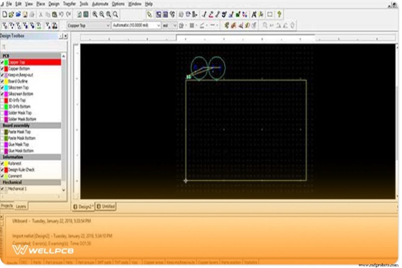
Creating a Board Outline
Define the board perimeter using one of the following methods:
- Drawing Tools – Use the asterisk (*) key to input coordinates manually.
- Import a DXF file.
- Use the Board Wizard for guided outline creation.
- From the toolbar, double‑click the Border Wizard icon.
- Delete any existing border to start fresh.
- Choose a multilayer or single‑layer stack‑up and click Next.
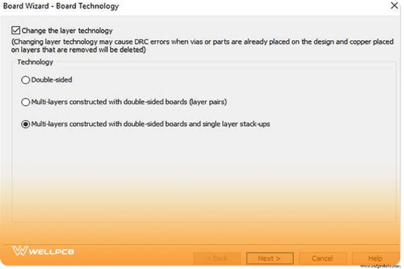
- In the Lamination Settings dialog, adjust as needed.
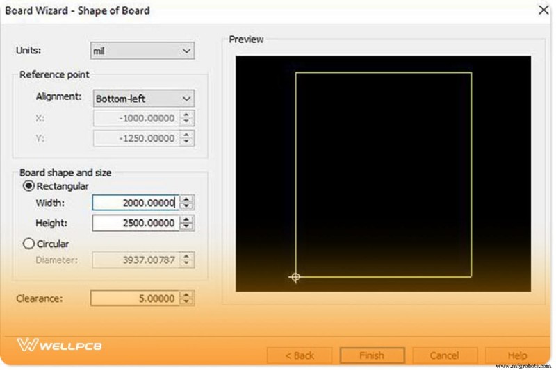
- Define the board shape: set the reference point to Left‑Bottom, choose Rectangular, and specify dimensions (e.g., width = 2500 mm, height = 2000 mm, clearance = 5 mm). Click Finish.
Editing the Border Outline
- To move the outline, double‑click Board Outline under the Layers tab and drag.
- To adjust the reference point, use the Options tab and edit the displayed box.
Placing Components
Components can be added by dragging from the database, using the spreadsheet view, importing a netlist, or employing the auto‑place feature.
Routing Traces
Ultiboard offers several routing options:
- Manual Trace – Use
LineorPolygontools to draw. - Follow‑Me Trace – Select two pins; the tool draws the path automatically.
- Connection Machine – Click
Place > Connection Machine, then click the start and end points. Ultiboard proposes routes; select one and confirm.
Preparing for Manufacturing
Cleanup
- Remove open trace ends:
Edit > Copper Delete > Open Trace Ends. - Delete unused vias:
Design > Clean Unused Vias.
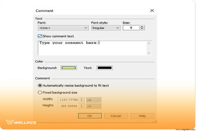
Adding Comments
Comments aid collaboration and provide manufacturing notes:
- Activate the comment layer via
Place > Comment. - Set text properties (font, size, background) and type your note.
- Click OK and double‑click the desired board spot to place the comment.
- To edit or delete, return to the comment dialog or press
Delete.
Exporting to Manufacturing
Export the design by pressing Ctrl‑E or selecting File > Export. The dialog allows you to choose Gerber, DXF, or other formats required by your manufacturer.
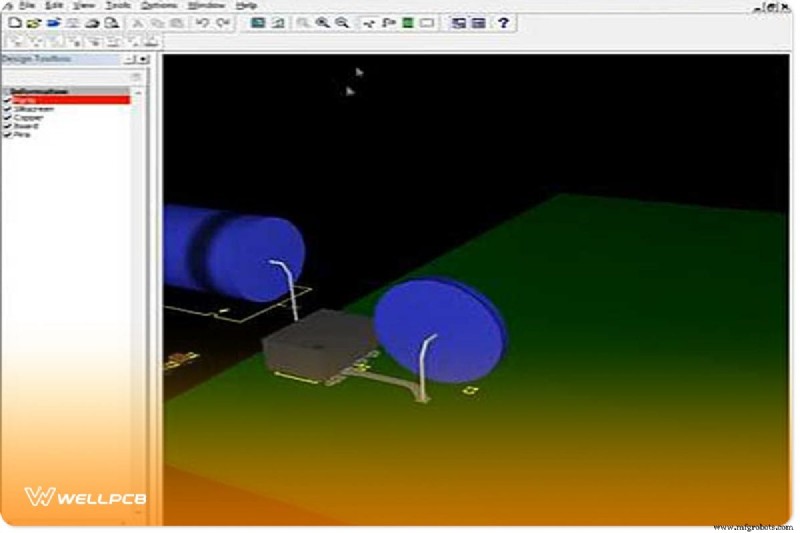
Viewing in 3‑D
Access the 3‑D viewer via Tools > 3D. Manipulate the view with mouse controls:
- Pan by clicking and dragging.
- Rotate by holding the cursor.
- Zoom with scroll wheel or
View > Zoom In/Out.
Advantages and Considerations
Benefits
- Intuitive, user‑friendly interface.
- Robust integration with spreadsheets and design rule checks.
- Fast export to industry standards (Gerber, DXF).
- Seamless transfer from Multisim schematics.
- Annotation tools help track design changes.
Limitations
- Steep learning curve for newcomers.
- Commercial license required; costs can reach $2,500 for the full suite.
When to Use Ultiboard
Ultiboard excels in projects requiring rapid layout, automated component placement, and efficient routing. Its integration with Multisim and the automated part placement features reduce repetitive tasks, making it a strong choice for both academic and professional environments.
Conclusion
Mastering Ultiboard transforms a concept into a tangible PCB ready for production. Whether you’re a student, hobbyist, or professional engineer, this guide equips you with the essential steps to design, validate, and export a board that meets industry standards.
For additional support, consider partnering with a reliable PCB fabrication service. Our turnkey solutions offer high‑quality, low‑cost manufacturing with fast turnaround. Contact us 24/7 for assistance.
Industrial Technology
- Accelerate Downtime Response with MachineMetrics: Boost Production & Operator Efficiency
- Key Factors That Predict Big Data Project Success
- Gas and Flame Safety: Protecting Workers in Power Generation
- Achieving Zero Defects: A Pragmatic Approach to Eliminating Failures
- Bill Lauer Retires from DVIRC, Signaling a New Era in Business Development
- Precision Measuring Tools: Harnessing Digital Metrology for Data-Driven Quality Control
- Designing a Bill of Materials (BOM) File: Proven Methods for PCB Production
- Mastering Business Intelligence: Crafting a Winning Strategy for Data-Driven Success
- Why California Is the Ideal Choice for Your Manufacturing Business
- Electric Pendulum: How Capacitors and Inductors Exchange Energy