


Single‑Sided PCB Design: A Cost‑Effective Solution for Low‑Density Electronics
What is a single‑sided PCB, and how can it enhance electronics? The answer lies in its simplicity and cost‑effectiveness, making it a valuable choice for many manufacturers.
What Is a Single‑Sided PCB?
Printed circuit boards can feature up to 20 conductive layers, each adding complexity and cost. A single‑sided PCB contains only one copper layer, eliminating shared circuit paths and dramatically simplifying the design process.
Because all traces run on the same side, the manufacturing steps are fewer, the tolerance window is larger, and the overall risk of design errors is reduced.
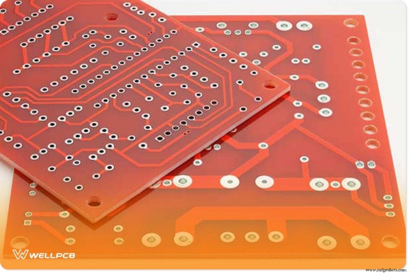
Stack‑Up of a Single‑Sided PCB
The typical stack‑up consists of a solder mask on both sides, a copper layer above the substrate, and the insulating substrate itself. This configuration protects the board from over‑current and mechanical stress.
Single‑ vs. Double‑Sided PCBs
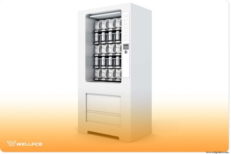
Both types use surface‑mount technology, but a double‑sided board offers top and bottom traces, enabling higher density circuits. In contrast, a single‑sided board is ideal for low‑density, non‑data‑intensive devices such as vending machines, simple appliances, and certain microwave controls.
Switching from a double‑sided to a single‑sided layout is often feasible with minor redesign, saving time and material costs without sacrificing performance.
Applications for Single‑Sided PCBs
Despite their long history, single‑sided PCBs remain relevant. Modern manufacturers use them for devices that do not require complex data pathways, including digital cameras, surveillance equipment, and even some HVAC controls.
Their straightforward construction makes them ideal for DIY projects and rapid prototyping, allowing designers to focus on functionality rather than board fabrication.
Exploring the Versatility of Single‑Sided PCBs
Beyond basic appliances, single‑sided boards power electronics such as air‑conditioning units and certain industrial controls. Their ease of manufacture and low cost are key factors driving their continued adoption.
Benefits of Single‑Sided PCBs
Switching to a single‑sided design offers tangible advantages:
Cost, Time, and Material Savings
With only one copper layer and a simple stack‑up, material usage drops dramatically, reducing both purchase cost and lead times.
Reduced Design Complexity
The absence of cross‑layer connections means fewer potential errors, easier troubleshooting, and a more intuitive design process.
Higher Production Reliability
Fewer layers translate to fewer steps in assembly, which lowers the chance of defects and simplifies quality control.
Cost Breakdown
A single‑sided PCB requires only four core components: substrate, copper layer, solder mask, and silkscreen. By contrast, double‑sided and multi‑layer boards add additional copper layers, prepreg, and drilling, inflating both cost and complexity.
Conclusion
Single‑sided PCBs are an underutilized asset in today’s electronics landscape. They excel in low‑density applications and can replace double‑sided designs in many cases with minimal redesign effort.
Ready to explore single‑sided solutions for your next project? Contact our experienced team to discover how we can help you achieve cost savings and faster time‑to‑market.
Industrial Technology
- Designing a Binary Half‑Adder: From Logic Gates to Ladder Diagrams
- Choosing the Right Chopper: A Comprehensive Guide to Types and Applications
- Investing in Tech: How Logistics Providers Can Modernize Operations
- Mastering Supply Chain Management: Five Essential Strategies Post-COVID
- Industry 4.0 & IoT in Germany: Current Landscape & Strategic Insights
- 4 Proven Strategies to Strengthen Supplier Relationships
- Swanton Welding – Premier Metal Fabrication Services in Griffin, Georgia
- MachineMetrics Secures $20M Series B to Expand Global Autonomous Machining Platform
- Choosing the Right Transistor Replacement: A Guide to Optimal Selection
- Critical Limitations of RFID in Military Asset Tracking