


Master PCB File Management: From Design to High‑Availability Manufacturing
Whether you’re a student navigating your first PCB project or a seasoned engineer scaling up production, the quality of your PCB files is the foundation of a successful build. This guide walks you through every step—from understanding file types to generating compliant Gerber data and ensuring your design meets manufacturer specifications.
PCB File Fundamentals
Every PCB design is represented by a collection of files that describe layers, routing, drill holes, and surface‑mount details. These files serve as the blueprint the manufacturer uses to fabricate your board.
What Is a PCB File?
A PCB file—typically with extensions like .brd (Eagle), .pcb (Altium), or Gerber variants—encapsulates all layer information, including copper traces, solder mask, silkscreen, and component footprints. It also contains metadata such as board dimensions and fabrication tolerances.
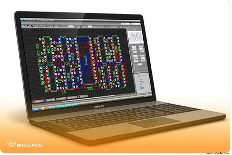
Figure 1 shows a typical PCB file opened in a design environment. The file provides the manufacturer with critical details: board outline, copper weight, dielectric thickness, and solder‑mask color.
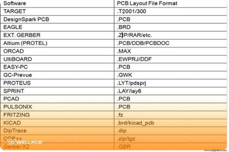
Common PCB File Formats
While the native design file is often proprietary, the industry standard for manufacturing is Gerber. Below is a quick reference to the most frequently encountered formats.
Table I – PCB File Formats
Generating Gerber Files with Popular CAD Tools
Gerber files provide a 2‑D artwork of your board, detailing copper, solder mask, and silkscreen layers. They do not carry net connectivity or design rule data, so it’s essential to follow the manufacturer’s instructions closely when exporting.
Figure 2 illustrates the Gerber export workflow in DipTrace. The process is similar across most EDA packages: define a manufacturing job, set layer selections, and run the CAM processor.
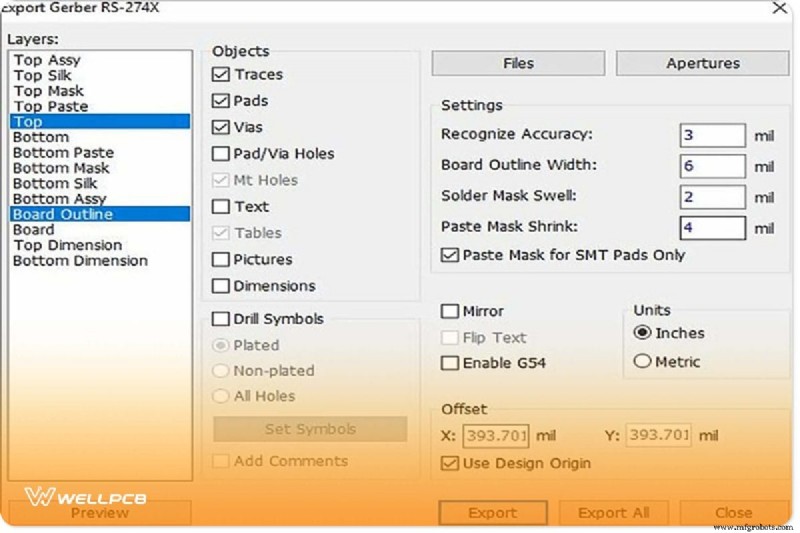
Typical steps for creating a Gerber set:
- Consult your manufacturer’s specification sheet for the exact file structure.
- Use the CAD tool’s CAM or Export wizard to generate the required layers.
- Validate the output with a Gerber viewer before sending to fabrication.
Opening and Inspecting PCB Files
Viewing a PCB File in Eagle
Eagle does not natively read .pcb files from other platforms. However, you can import designs via a script or by converting to an Eagle-compatible format such as .brd. A popular method is to use the Eagle import script available from community forums.

Using a Gerber Viewer
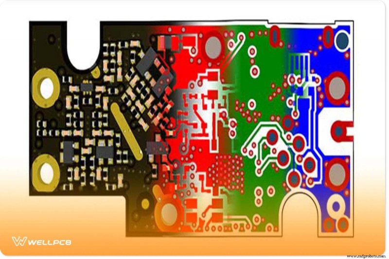
Before submission, always preview each layer in a Gerber viewer. This step catches missing traces, mis‑aligned silkscreen, or incorrect drill holes. Figure 4 demonstrates a typical Gerber preview.
Cross‑Platform File Conversion
From Eagle to Gerber
With a .brd file open:
- File > CAM Processor.
- File > Open > Job, then load
gerb274x.camfrom Eagle’s default CAM folder. - Click Process Job to generate the full Gerber set.
For a deeper dive, see our Hands‑On The Gerber File article.
Altium to Eagle
Export the Altium design as an ACCEL ASCII file (.acc) and import it into Eagle via Import > File > Pad. The importer translates the netlist and footprints into Eagle’s schema.
Converting Gerber to Altium
Altium recognises Gerber layers by their extensions: GTL for top, GBL for bottom, GTO for outer copper, etc. Simply rename your Gerber files accordingly and let Altium import the set.

Manufacturer File Requirements
Gerber File Checklist
- Drill tool list & Excellon drill files
- All copper layers with correct polarity
- Solder mask and silkscreen layers
- Aperture (D‑code) list
- Board outline and edge cuts
- Readme with layer naming conventions
- Copper weight and dielectric thickness specifications
Native Design Files Accepted by Some Manufacturers
- Altium (Protel)
.pcb - EAGLE
.brd - Ultiboard
.u3 - OrCAD
.pcb - PCB123
.sch/.brd - IVEX
.ivx
Drill File Specifications
- Prefer Excel or plain‑text format.
- Exclude G‑code prefixes like G01, G54, and D commands.
- Use ASCII text; no binary or graphic artifacts.
- Include tool reports and NC drill files for plated features.
- Separate plated and non‑plated holes on appropriate layers.
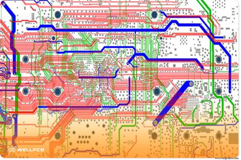
Routing and Design Rule Guidance
Manufacturers often recommend a copper backset of 0.020″ to protect trace edges. While some may allow irregular shapes, constraints on minimum width and spacing still apply. Figure 5 illustrates a typical routed board layout.
Conclusion
High‑quality PCB files are the key to a smooth manufacturing process. By understanding file formats, adhering to manufacturer specs, and rigorously validating each layer, you can avoid costly re‑works and production delays.
Need help preparing your files or verifying compliance? Our experienced engineering team is ready to assist—contact us today.
We value your feedback and are always eager to support your next project.
Industrial Technology
- Understanding Voltage and Current: The Foundations of Electrical Flow
- Choosing the Right LED Strip Lights: A Practical Guide
- ERP Software Series: Crafting Comprehensive User Requirements
- World’s Tiny House: A 20‑Micrometer Microstructure
- Shaping Tomorrow: Fast Radius' Vision for Cloud Manufacturing
- Hardness Testing Techniques: Rockwell & Brinell Methods
- Preparing Tomorrow’s Workforce for Industry 4.0: Training Strategies for the Digital Factory
- How Cutting-Edge Electronics Drive Innovation Across Industries
- Secure Your Supply Chain: Strategies to Counter Cybercrime, Natural Disasters, and More
- DVIRC Secures Second DOD-OEA Contract to Empower SMMs in Advanced Manufacturing