


The Complete PCB Design & Manufacturing Playbook – From Concept to Delivery
Printed Circuit Boards (PCBs) remain the backbone of modern electronics, enabling the dense integration of complex circuits in a compact footprint. Their role is indispensable in devices ranging from smartphones to wearables.
Achieving a reliable, high‑performance board requires meticulous attention to heat management, electromagnetic interference, impedance control, and mechanical integrity. Every phase—from schematic capture and layout to fabrication and assembly—must be executed with precision to ensure the final product meets stringent quality and reliability standards.
Chapter 1: PCB Design and Layout
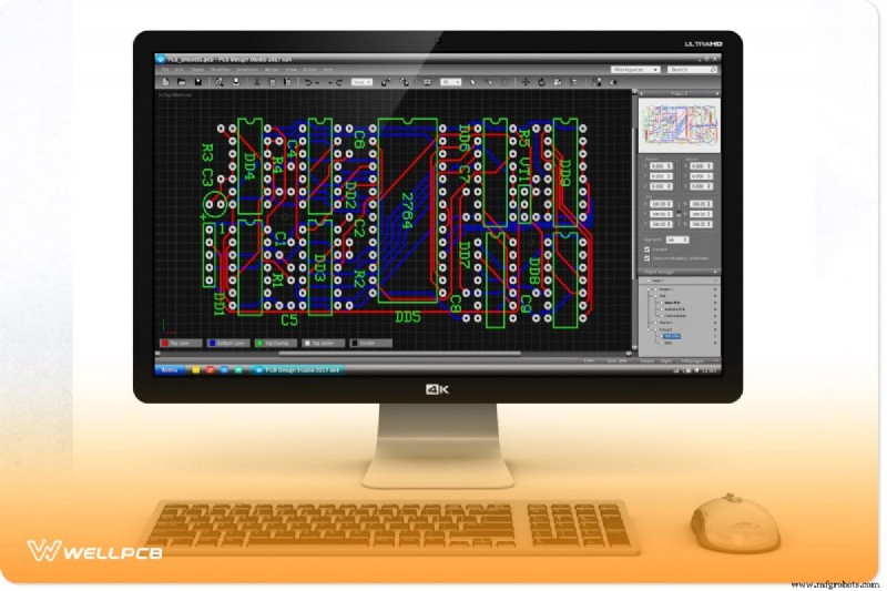
1.1 Selecting the Right Design Software
The foundation of a successful PCB project starts with the right design tool. A robust CAD solution should streamline routing, via placement, and design rule enforcement, while offering a comprehensive component library and advanced simulation capabilities.
- Accurate trace routing and via definition
- Integrated design rule checks (DRC & ERC)
- Support for multi‑layer designs and high‑speed signal integrity analysis
- 3‑D visualization for both bird’s‑eye and close‑up inspection
- Seamless integration with external CAD systems and file formats
Top‑tier options such as Altium Designer, Autodesk Eagle, and DipTrace deliver these features, balancing power and usability. When choosing, prioritize feature set over a steep learning curve, then evaluate cost‑effectiveness and licensing flexibility.
1.2 Key Layout Considerations
Board Size & Component Placement
Board dimensions must align with the target product’s form factor and functional requirements. For wearables or compact modules, space constraints demand tighter layouts, whereas larger consumer electronics allow more generous footprints.
Strategic component placement is crucial for manufacturability:
- Align similar components (e.g., transistors) to simplify assembly and inspection.
- Account for component height and footprint to prevent mechanical interference and ensure smooth wave‑soldering.
- Reserve ample routing space around high‑pin devices to avoid congestion.
Signal Routing Best Practices
Efficient routing preserves signal integrity and manufacturability:
- Manual oversight of auto‑routing: Verify that auto‑routing decisions do not compromise power, ground, or high‑speed paths.
- High‑speed routing: Use solid ground planes, maintain uniform trace widths, and employ vias strategically to avoid impedance discontinuities.
- Daisy‑chain buses: Consolidate identical component connections to reduce clutter, but account for added propagation delay.
- Dedicated power/ground planes: Provide low‑impedance return paths and shield sensitive signals from EMI.
Design Rules & Guidelines
Establishing clear Electrical Rule Checks (ERC) and Design Rule Checks (DRC) early guarantees a manufacturable design. Define trace widths, clearances, via specifications, and high‑speed parameters to catch issues before fabrication.
1.3 Stack‑Up & Material Selection
The stack‑up defines electrical performance, mechanical strength, and thermal behavior. A typical multi‑layer board alternates copper, dielectric, and solder‑mask layers, topped with a silkscreen.
Choosing Materials for Thermal & Cost Efficiency
FR‑4 remains the industry standard due to its cost‑effectiveness, though it offers limited thermal conductivity. For high‑power or heat‑sensitive components, consider:
- Metal core (Aluminum): Excellent heat dissipation and structural support.
- Ceramic (Alumina or Aluminum Nitride): Superior thermal performance but higher cost.
Balancing thermal needs with budget constraints is key to an optimal stack‑up.
1.4 Vias & Thermal Management
Via Types and Their Applications
Vias—whether through, blind, or buried—connect layers and transfer current and heat. Consistency in via size and placement improves manufacturing yield and electrical reliability. Consult with your PCB fabricator to match via specifications to the board’s thermal and current requirements.
Managing Thermal Challenges
High‑density boards generate significant heat. Mitigate this by:
- Placing heat‑sinking vias or thermal vias near hot components.
- Using heat sinks, fans, or thermal relief pads where appropriate.
- Ensuring adequate clearance around high‑temperature parts to allow airflow and soldering processes.
Chapter 2: Generating Gerber Files
2.1 What Gerber Files Are
Gerber files are the de‑facto standard for PCB manufacturing, encoding each board layer as a 2‑D vector image. They accompany drill files to produce the final etched board. Today, ~90% of PCB jobs rely on Gerber 274‑X and Excellon drill data.
Creating Gerbers with Eagle 3.55
Follow these streamlined steps:
- Open your board file in Eagle.
- Run the DRILLCFG.ULP to generate drill data.
- Launch the CAM Processor and load GERBER.CAM.
- Process the job—accept prompts regarding dummy files and multiple signal layers.
- Collect the generated files (e.g., .WHL, .CMP, .SOL, etc.), zip them, and send to your manufacturer.
Generating Gerbers in Altium Designer
- Navigate to File > Fabrication Outputs > Gerber Files.
- Set measurement units and layer selections (e.g., uncheck G1–G3 for a 2‑layer board).
- Enable Embedded Apertures for cleaner files.
- Click OK to export.
2.2 File Extensions & Viewing Tools
Gerber files typically use the .gbr extension, though .gbx, .top, and .bot are also common. A dedicated viewer is essential for verifying layer alignment, clearances, and overall design integrity.
- Online Gerber Viewer – Supports Gerber 274X and Excellon, with zoom and layer‑toggle features.
- EasyEDA Gerber Viewer – Offers layer isolation, color selection, and statistical analysis of holes and dimensions.
- Numerical Innovation Gerber Viewer – Robust compatibility, precision zoom, and seamless integration with Eagle/Altium exports.
2.3 Common Gerber Pitfalls & Prevention
Typical errors include:
- Misaligned or missing layers
- Insufficient pad/traces clearances
- Obsolete file formats or unit mismatches
- Duplicate or overlapping objects
- Incomplete or corrupted files
Best practices:
- Conduct thorough design reviews before export.
- Use dedicated viewers to validate every layer.
- Leverage built‑in DRC/DRC checks.
- Adhere to naming conventions and consistent units.
- Verify drill files for accuracy.
- Maintain version control and collaborate closely with your manufacturer.
Chapter 3: PCB Fabrication Process
The manufacturing journey encompasses six critical stages:
3.1 Pre‑Production Engineering
Engineers review the design documents, confirm completeness, and generate an accurate quotation. This step ensures all manufacturing requirements are documented and potential issues flagged early.
3.2 Lamination & Imaging
- Cut Lamination: Tailor board size and panel geometry.
- Drying: Remove moisture at 150 °C for 3–4 h to prevent warping.
- Inner Layer Imaging: Apply dry film, expose, and develop to reveal copper traces.
Subsequent chemical etching removes unprotected copper, leaving the desired trace patterns.
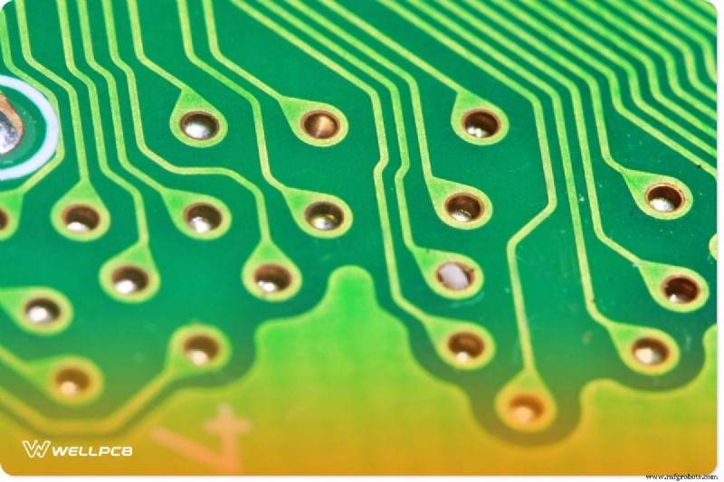
3.3 Drilling & Plating
Drilling—laser or mechanical—creates vias and through‑holes. Laser drilling offers precision for microvias, blind, and buried vias. Plating follows with Electroless Copper Deposition (ECP) for thin initial layers and Horizontal Electrolytic Plating (HEP) for thicker copper paths.
3.4 Outer Layer Imaging & Etching
Dry film is applied to the outer copper surface, exposed, and developed. The copper under the film is protected during this stage, ensuring accurate trace formation.
3.5 Solder Mask & Silkscreen
After UV exposure, a liquid solder mask shields copper from oxidation and corrosion. Silkscreen printing then adds critical component identifiers and assembly instructions.
3.6 Surface Finish & Profiling
Surface finishes such as ENIG, HASL, Lead‑Free HASL, and OSP provide solderability and durability. Compliance with RoHS mandates lead‑free solutions for EU markets. Profiling shapes the board edges to the customer’s specifications.
Chapter 4: Final Testing & Quality Control
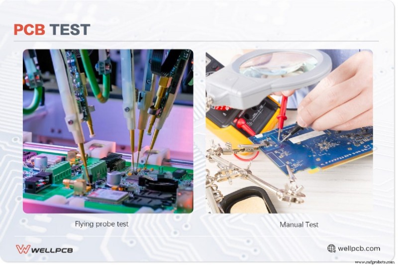
Image: PCB Test
4.1 Electrical Testing
Electrical reliability is verified through continuity, isolation, and Flying Probe testing. These checks confirm that all nets are complete, free from shorts, and meet the design’s electrical specifications.
4.2 Visual Inspection & Packaging
Our quality team performs a meticulous visual inspection, measuring dimensions, hole counts, and warpage. Successful boards receive a test report and are vacuum‑sealed to protect against dust and moisture before secure packaging and global shipping via DHL or FEDEX.
Conclusion
PCB design and manufacturing are foundational to reliable electronics. By mastering layout fundamentals, stack‑up choices, precise Gerber creation, and rigorous fabrication processes, you ensure longevity and performance.
We offer expert design review, fabrication support, and ongoing communication to refine your project before production.
Ready to elevate your PCB workflow? Contact us today and let’s bring your design to life.
Industrial Technology
- Casting vs Forging: Key Differences and Applications
- Strengthening Supply Chains During COVID-19: Three Proven Strategies
- Vision Inspection Systems: Driving Accuracy & Efficiency in Metrology
- A Comprehensive Overview of the Evolution of Electrical Design
- Vertical vs. Horizontal Green Sand Casting: Choosing the Optimal Process for Efficiency and Cost
- Intel’s Stacey Shulman Highlights Edge Insights, Cloud, and AI at MWC Barcelona
- Build an LED Scanner in 4 Easy Steps: A Practical Guide
- Cut CNC Machining Costs: Proven Strategies to Reduce Time and Save Money
- Alternative Energy Powers Reliable Vaccine Cold Chains
- Mastering Sheet Metal Notches & Tabs: Design Tips for Precision Parts