


Choosing the Right PCB Material: Design Criteria & Material Selection
In PCB manufacturing, choosing the correct substrate material is critical for performance, reliability, and cost. The vast array of options—each with distinct electrical, thermal, and mechanical properties—requires careful evaluation. This guide explains the key factors that drive material selection and offers practical advice for designers.
PCB Construction Basics
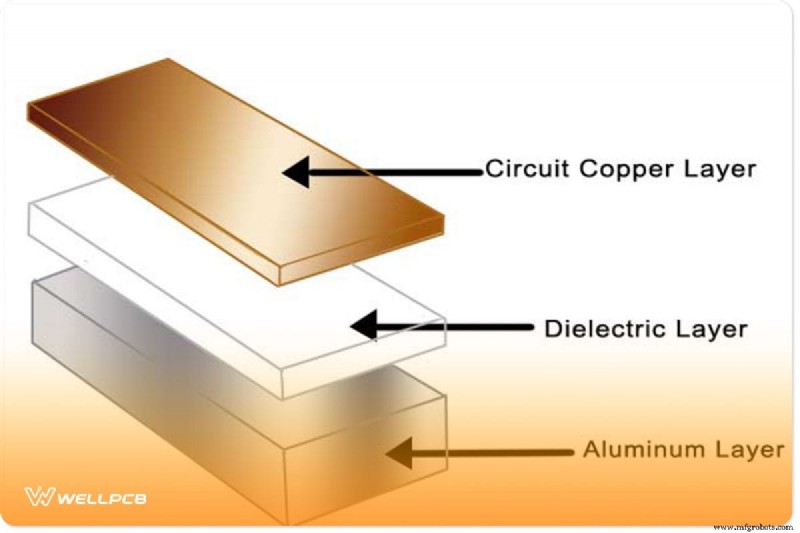
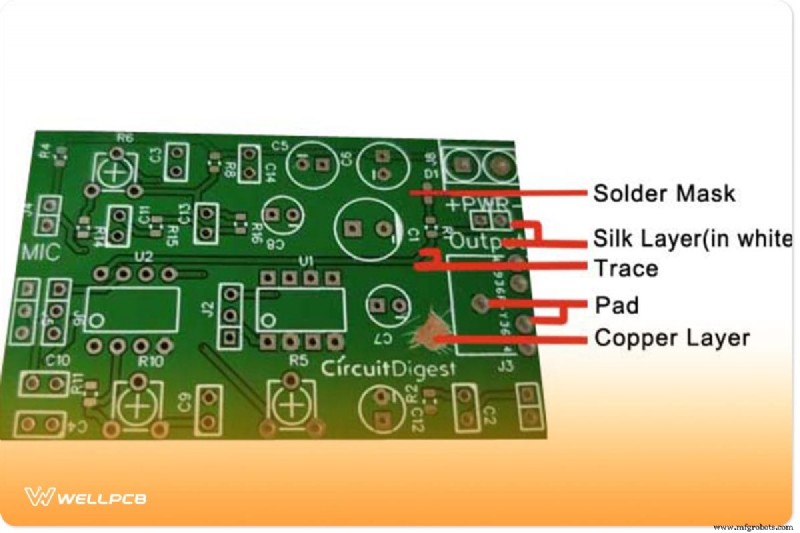
Modern PCBs are typically built from three core layers:
- Circuit Layer: Copper traces, usually 1–10 oz, carry signals and power.
- Insulating Layer: A dielectric that isolates copper from the base, providing both electrical isolation and thermal conductivity.
- Base Layer: Often aluminum or copper‑clad substrates. Aluminum is favored in high‑power designs for its superior heat dissipation and mechanical robustness.
When selecting a base, heat dissipation, mechanical strength, and cost must be balanced. Aluminum substrates—especially 1 mm thick—offer an excellent compromise for demanding power electronics.
Insulating Layer
A dielectric material resists electrical conduction while allowing heat transfer. Common dielectrics include porcelain, mica, glass, certain plastics, and metal oxides.
The lower the dielectric loss, the more efficient the material.
Excessive electric field can cause dielectric breakdown, turning the material into a conductor. Selecting a material with a high breakdown voltage mitigates this risk.
PCB Substrate Fundamentals
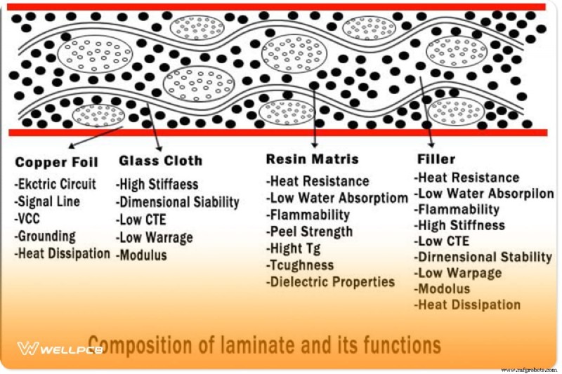
PCBs typically comprise an upper and lower layer. The substrate—usually a composite of epoxy and glass fibers—determines the board’s mechanical integrity and electrical performance.
Global substrate demand approaches 51 million square meters annually.
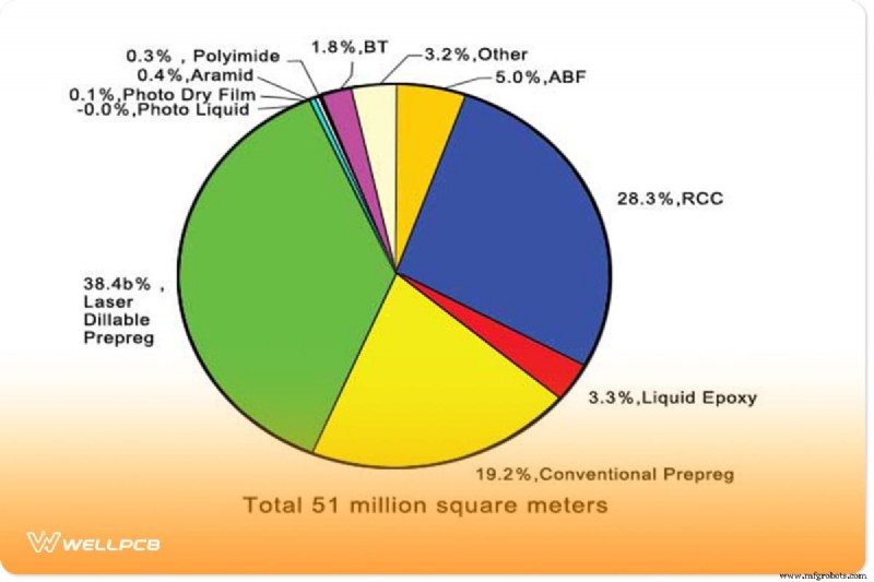
Most substrates combine epoxy with a BT (butyl‑trifluoroethylene) mixture, reinforcing the dielectric stack with metal foil to achieve the desired impedance.
The chart below summarizes common substrate options and their typical applications:
Common PCB Material Classes
Three primary material families are widely used:
• Non‑woven glass – Glass microfibers dispersed in resin; suitable for high‑frequency layers but with limited mechanical robustness.
• Woven glass – Glass cloth woven into the substrate; offers good mechanical strength but may underperform in multilayer thermal management.
• Filled – Contains ceramic or other fillers to raise the dielectric constant; ideal for precision impedance control.
Aluminum PCBs
Aluminum substrates (often called “IMS” PCBs) integrate a copper layer, a thermally conductive resin, and a top copper foil. Standard dimensions are 1.6 mm board thickness, 100 µm ceramic isolation, and 35 µm copper.
Variants:
- Flexible aluminum
- Hybrid copper‑core
- Multilayer aluminum
- Through‑hole aluminum
Benefits include low cost, lightweight construction, excellent thermal management, mechanical rigidity, and superior EMI shielding.
Typical applications:
- High‑power switching and LED drivers where heat dissipation is critical.
- Automotive and RF modules that demand lightweight, durable boards.
- Any design where integrated heat sinking is required.
FR‑4
FR‑4—short for Flame‑Retardant Grade 4—is a glass‑reinforced epoxy laminate that has become the industry standard for most PCBs.
Key properties:
- Dielectric constant (εr) ≈ 4.4
- Dielectric strength ≈ 5 MV/m
- Breakdown voltage ≈ 50 kV
- Glass transition temperature (Tg) ≈ 140 °C
FR‑4 replaces the older G‑10 material due to its self‑extinguishing qualities. It balances cost, manufacturability, and performance for both low‑ and high‑frequency applications.
Limitations:
- Dielectric constant varies between lots and with frequency.
- Loss tangent increases at higher frequencies.
- Lead‑free reflow temperatures can affect thermal conductivity.
For high‑current designs, use thicker copper (≥1 oz). The default board thickness remains 1.6 mm.
High‑frequency circuits (RF, microwave, antennas) typically employ low‑loss dielectric materials rather than standard FR‑4.
Common advantages of FR‑4:
- Widely available and economical.
- High Tg (130–170 °C).
- Halogen‑free and lead‑free compatible.
FR‑1, FR‑2, CEM‑1, CEM‑3
These substrates are cheaper alternatives for single‑ or double‑layer boards:
- FR‑1/FR‑2 – Phenolic paper composites with low Tg; ideal for low‑frequency, single‑layer circuits.
- CEM‑1 – Paper‑glass‑epoxy; typically used in single‑sided boards.
- CEM‑3 – Glass‑epoxy; common in double‑sided boards; cheaper than FR‑4.
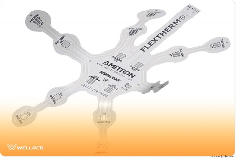
Polyimide
Polyimide is the material of choice for flexible PCBs. It offers excellent electrical stability across 200–300 °C and maintains mechanical flexibility.
Pre‑preg
Pre‑preg (pre‑impregnated) is fiberglass woven with partially cured resin. When heated, it bonds layers together, providing mechanical strength and electrical insulation. Variants (SR, MR, HR) differ in resin content and glass‑transition temperatures.
Selecting the Right PCB Material
Choosing a substrate requires understanding the design’s thermal, electrical, and mechanical demands. Below are the critical criteria.
Thermal Properties
Thermal Conductivity (k)
Measured in W/m·K, this metric indicates how efficiently a material dissipates heat. Typical dielectrics range from 0.3 to 6 W/m·K; copper reaches 386 W/m·K.
Decomposition Temperature (Td)
The temperature at which a substrate permanently degrades. Select materials with Td > 250 °C to accommodate soldering (200–250 °C) while keeping Tg below that range.
Glass Transition Temperature (Tg)
The temperature at which the substrate softens. It must remain above the maximum operating temperature to avoid deformation.
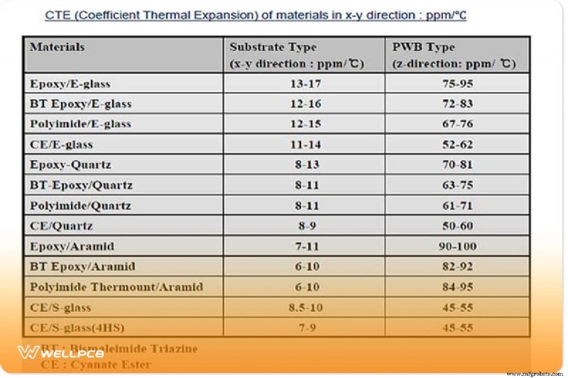
Coefficient of Thermal Expansion (CTE)
Expressed in ppm, CTE represents dimensional changes with temperature. A typical acceptable range is 10–20 ppm; overall CTE should be ≤ 70 ppm to reduce stress between copper and substrate.
Electrical Properties
Dielectric Strength
Indicates the maximum voltage the material can withstand in the Z direction, usually 800–1500 V/mil.
Volume Resistivity
Measured in ohm‑cm, values > 10 MΩ·cm are preferred to prevent leakage.
Surface Resistivity
Measured in MΩ/sq; typical values range from 10³ to 10⁹ MΩ/sq.
Loss Tangent (tan δ)
Lower values (0.001–0.02) mean less power loss, especially at high frequencies.
Dielectric Constant (εr)
For high‑frequency work, a stable εr between 3.5 and 5.5 is ideal.
Heat & Power Considerations
- Moisture Absorption – 0.01–0.20 % limits dielectric performance.
- Flammability (UL94) – Must not sustain flaming combustion for more than 10 s.
- Methylene Chloride Resistance – Chemical resistance measured at 0.01–0.20 %.
Mechanical Properties of Flex & Flex‑Rigid Boards
- Density – g/cm³ or lb/in³.
- Peel Strength – Bonding strength between copper and dielectric.
- Time to Delamination – Durability under thermal or moisture stress.
- Flexural Strength – Measured in PSI or MPa; assessed via central load or Young’s modulus.
Additional Design Factors
Board Thickness
Thicker boards provide structural support for heavy components. Standard copper thickness is 35 µm (1 oz); thicker copper (≥1 oz) is advisable for high‑current traces.
Track Spacing
Maintain a minimum spacing of 2 mm for power traces and 1 mm for signal traces to mitigate crosstalk.
Via Quality
Filled or balled vias prevent solder wicking and ensure reliable electrical contact, especially in BGA packages.
Cost vs. Performance
High‑frequency boards often require low‑loss dielectrics, which can be pricey. Balance cost against performance to achieve a durable, cost‑effective design.
Conclusion
Understanding the interplay between thermal, electrical, and mechanical properties enables designers to select the optimal PCB material for any application. Whether you need the lightweight heat‑sinking of aluminum, the cost‑effectiveness of FR‑4, or the flexibility of polyimide, the right choice will extend reliability and performance.
WellPCB offers top‑tier manufacturing and assembly services using industry‑leading materials such as FR‑4, Rogers, and high‑performance polyimides. Our experienced team delivers boards that meet the most demanding specifications.
For further guidance on PCB material selection, contact our support team at sales@wellpcb.net.
Industrial Technology
- Side-Emitting LED Strips: Energy‑Efficient, Versatile Lighting for Any Space
- Top 4 Qualities Manufacturers Must Seek in New Hires
- Global Water Crisis: The Critical Shortage Threatening Humanity
- Understanding Op‑Amp Input Impedance: Definition, Significance, and Calculation Guide
- Rising Efficiency: Revolutionizing Mechanical Transmissions
- Advanced 2.5 & 3-Axis Milling Solutions for Complex Projects
- Investment Casting: Unlocking Cost Savings and Quality – Part 2
- Plastic Injection Molding: Material Choices and Optimal Applications
- Exponent Rules: Key Properties for Algebraic Manipulation
- Understanding Flexible Resin: Properties, Uses, and Best Practices