


From Breadboard to Production: Expert Guide to Scaling PCB Prototypes
Transforming a breadboard prototype into a production‑ready PCB demands a blend of creativity, disciplined methodology, and hands‑on expertise. While the timeline varies for each project, the process follows clear milestones that guide you from concept to commercial release.
Building Your First PCB Prototype
Once you’ve validated a proof‑of‑concept (PoC), the next step is to create a manufacturable prototype. A hand‑built PCB prototype is a compact, testable version of the final product that lets designers validate electrical performance and mechanical layout before committing to larger runs.
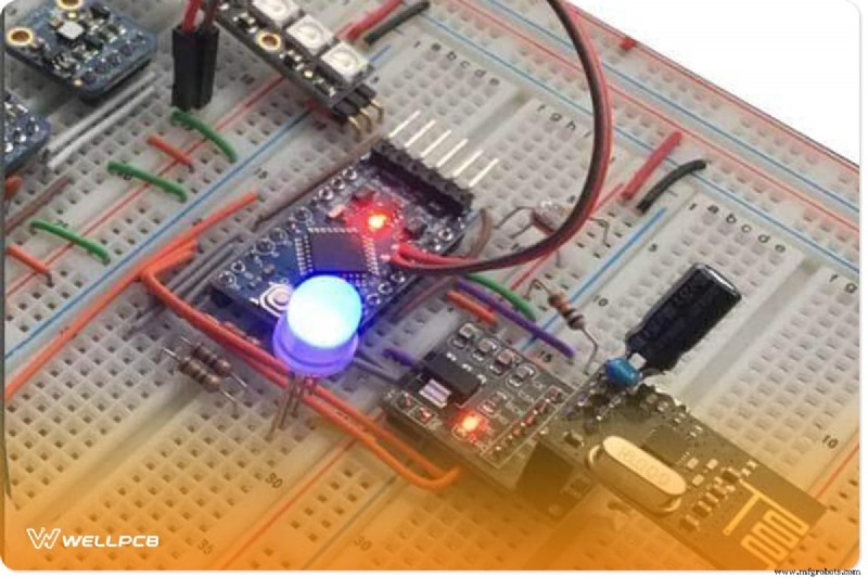
Today’s free tutorials and abundant component libraries make it possible to fabricate a functional prototype in a few hours. However, moving from a prototype to a mass‑produced product requires careful planning and industry‑standard practices.
Decisions about hardware design cascade into software choices, impacting the entire product lifecycle. While hobby platforms like Raspberry Pi or Arduino are great for rapid experimentation, they often lack the scalability, cost‑efficiency, and reliability needed for commercial production.
Many hardware startups start with Arduino boards because of their ease of use and large community support. Yet, for a production‑grade device, you’ll need to transition to a custom PCB with components sourced from reliable suppliers such as Digi‑Key, Mouser, Arrow, or Adafruit.
Choosing the Right Components
The first step is to compile a bill of materials (BoM) based on your block diagram and functional requirements. For example, a wearable heart‑rate monitor might need:
- A microcontroller (e.g., Atmega, ARM Cortex‑M, PIC)
- A pulse sensor (dedicated module or LED/photodiode pair)
- Power management circuitry
- A display interface (LCD, OLED, TFT)
Component procurement can be streamlined by using a single supplier or a curated list of trusted vendors. AliExpress can be useful for prototypes, but for consistency and quality, Digi‑Key or Mouser are preferred.
Creating the Schematic
A schematic diagram is the blueprint of your circuit. It captures every connection and is the foundation for PCB layout. Use a professional CAD tool—KiCAD (free), Eagle CAD, Altium Designer, DipTrace, or OrCAD—to build and verify your schematic.
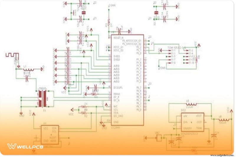
Follow these best practices to keep your schematic clean:
- Use junction dots for shared nodes.
- Assign net names instead of drawing individual traces.
- Maintain consistent symbols for identical components.
- Divide complex designs into logical blocks.
After final verification, export the schematic for PCB layout generation.
Designing the PCB Layout
The PCB layout translates the schematic into a physical board. It determines cost, performance, durability, and manufacturability. Key considerations include:
- Board size and shape
- Layer count and stack‑up
- Trace width, spacing, and clearance
- Component placement and routing of high‑speed or high‑power signals
- Thermal management and impedance control
Use the same CAD tool to switch from schematic to layout view. The software will auto‑populate footprints based on your component library.
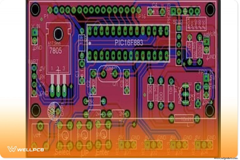
After routing, run Design Rule Checks (DRC) and Electrical Rule Checks (ERC) to catch violations early. Once validated, generate Gerber files for manufacturing.
Manufacturing Your PCB with WellPCB
WellPCB is a trusted partner for rapid PCB prototyping and small‑batch production. They accept Gerber, PCB, PCBdoc, and CAM files and provide free silkscreen on both sides.
Key specifications to keep in mind:
- Minimum trace/space: 4 mil
- Line width: 4 mil (or 3 mil for high‑density boards)
- Silkscreen colors: white, yellow, black (RoHS‑compliant inks)
- Board thickness: 0.2–6.0 mm
- Finish: HASL, ENIG, OSP, or lead‑free options
Order steps:
- Visit the WellPCB online quote.
- Enter board details and add to cart.
- Register an account and upload your Gerber files.
- Review the free DRC report and confirm the order.
- Receive production lead times: 24 h for 2‑layer boards, 48 h for 4–8 layers, and 120 h for 10+ layers.
WellPCB also offers assembly services (SMT/TH) and can source components on your behalf, streamlining the transition from prototype to finished product.
Transitioning to PCB Assembly (PCBA)
Once the PCB is fabricated, the next phase is component assembly. For small runs (<10 units), hand soldering may suffice, but for larger volumes, automated pick‑and‑place and reflow processes deliver higher quality and consistency.
WellPCB’s assembly service supports:
- Surface‑mount device (SMD) placement
- Through‑hole component (THC) insertion
- Final inspection and functional testing
- Optional programming of MCUs and firmware loading
To request a quote, submit a Bill of Materials (BoM) and component placement files through the PCB Assembly portal. WellPCB’s average turnaround for high‑volume orders is 25 days, with expedited options available.
Cost‑Saving Strategies for Prototyping and Production
Optimizing cost from the outset saves time and money during large‑scale manufacturing. Consider these tactics:
- Minimize board area to reduce copper and substrate usage.
- Prefer SMD components to eliminate drilling and reduce board size.
- Design for panelization to allow multiple boards on a single panel, cutting assembly time.
- Use standard silkscreen colors and avoid custom artwork to lower turnaround.
- Avoid unnecessary via types (blind/buried) unless required for high‑density designs.
- Choose a reputable manufacturer with transparent pricing and quick DRC checks.
Applying these principles can reduce production costs by thousands of dollars, especially in high‑volume runs.
Final Considerations for Market Launch
Beyond design and manufacturing, successful product deployment requires:
- Compliance certifications (FCC, CE, RoHS, etc.) for wireless devices.
- Protective enclosures that match the product’s form factor and aesthetics.
- Robust quality control processes, including inspection reports and batch traceability.
- Continuous improvement loops to refine design and manufacturing over successive runs.
With a reliable partner like WellPCB and a disciplined design workflow, you can confidently move from a simple breadboard prototype to a polished, market‑ready product.
Industrial Technology
- How Parcel Shippers Can Weather Peak‑Season Rate Hikes: 5 Proven Strategies
- How Cutting Quotes Can Revolutionize Your Pricing Strategy – A Complete Guide
- Optimizing Pump Repairs: How to Make the Most of Extra Goulds Parts
- Transforming Post-Pandemic Retail with RAIN RFID: Enhanced Visibility and Flexibility
- Build a Potato Battery: A Step‑by‑Step Guide to DIY Electrochemical Power
- Apple Unveils the 2019 Mac Pro – Key Design and Performance Highlights
- Essential Guide to Utility Asset Management: Mastering Asset Categorization
- Dielectric Strength of Insulators – Key Data for Electrical Engineers
- EV Boom Reshapes Auto Supply Chains: Tackling Lithium Shortages
- Warehouse-Level Disruptions: The Hidden Catalyst of Supply Chain Turbulence