


PCB Trace Thickness: Key Considerations for Reliability and Performance
Printed Circuit Boards (PCBs) are the foundation of virtually every modern electronic device. The copper traces that carry current across a PCB are more than mere conductors; their thickness directly influences current‑carrying capacity, thermal performance, mechanical robustness, and ultimately the reliability of the finished product.
Inconsistent or insufficient trace thickness can trigger overheating, voltage drops, or even sparking—risks that compromise not only the PCB but also the components mounted on it. For PCB designers, selecting the correct, uniform copper thickness is therefore non‑negotiable.
Typical Trace Thickness Ranges
Trace thickness is measured in ounces of copper per square foot, which is easily converted to inches or millimetres. Standard trace thicknesses (based on IPC‑4562) span from 0.008″ (0.2 mm) to 0.240″ (6 mm). Commonly used values include:
- 0.2 mm (0.0079″)
- 0.4 mm (0.016″)
- 0.5 mm (0.020″)
- 0.6 mm (0.024″)
- 0.8 mm (0.032″)
- 1.0 mm (0.040″)
- 1.2 mm (0.047″)
- 1.5 mm (0.062″)
- 1.6 mm (0.063″)
- 2.0 mm (0.079″)
- 2.3 mm (0.091″)
These values cater to different power levels, board density, and mechanical requirements.
Trace Thickness by Layer and Copper Weight
Four‑layer PCBs typically employ one of the following trace thicknesses: 0.020″, 0.031″, 0.040″, 0.047″, 0.062″, 0.093″, or 0.125″. Inner layers may use ½ oz., 1 oz., or 2 oz. copper foil, chosen to meet current‑carrying and impedance criteria.
Copper Weight Specification Table
| Weight | Absolute Cu Min. (IPC‑4562 minus 10%) (µm [µin]) |
Maximum Processing Allowance (µm [µin]) |
Minimum Final Finish (µm [µin]) |
|---|---|---|---|
| 1/8 oz. [5.10] | 4.60 [181] | 1.50 [59] | 3.1 [122] |
| 1/4 oz. [8.50] | 7.70 [303] | 1.50 [59] | 6.2 [244] |
| 3/8 oz. [12.00] | 10.80 [425] | 1.50 [59] | 9.3 [366] |
| 1/2 oz. [17.10] | 15.40 [606] | 4.00 [157] | 11.4 [449] |
| 1 oz. [34.30] | 30.90 [1,217] | 6.00 [236] | 24.9 [980] |
| 2 oz. [68.60] | 61.70 [2,429] | 6.00 [236] | 55.7 [2,193] |
| 3 oz. [102.90] | 92.60 [3,646] | 6.00 [236] | 86.6 [3,409] |
| 4 oz. [137.20] | 123.50 [4,862] | 6.00 [236] | 117.5 [4,626] |
The table above outlines the minimum copper thickness required, the permissible processing margin, and the final finish you can expect for each copper weight. These figures are critical when designing high‑density or high‑current boards.
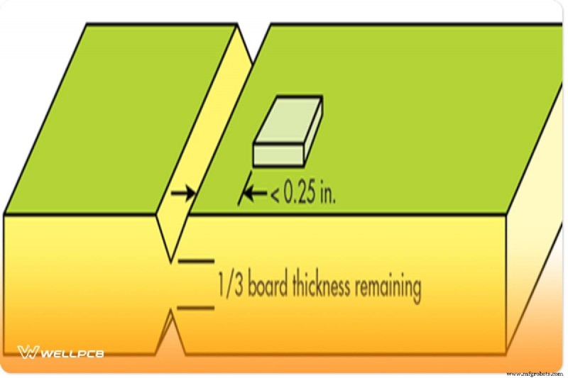
Illustrations of Thickness Variations
Figure 1 demonstrates how copper thickness changes before and after the etching process, affecting the residual copper profile.
Figure 2 depicts the relationship between copper thickness, etching depth, and the remaining board thickness—key for predicting trace integrity and mechanical strength.
Frequently Asked Questions
- What is PCB trace thickness? The vertical dimension of the copper layer that forms the conductive path on a PCB.
- How is it calculated? By combining trace width, copper weight, and the current rating of the circuit. Design tools or calculators streamline this process.
- Why is it important? Proper thickness prevents overheating, voltage drops, and enhances reliability. Incorrect values can cause component failure.
- Common standards? Typical values include 0.020″, 0.031″, 0.040″, 0.047″, 0.062″, and 0.093″, chosen based on application needs.
- How to choose the right thickness? Base your decision on the current requirement, trace width, and copper weight. Use a trace calculator to validate the design.
Conclusion
Trace thickness is as pivotal to a PCB as its overall layout. Accurate calculations, adherence to industry standards, and the use of reliable design tools are essential to deliver high‑performance, safe, and cost‑effective boards. By optimizing copper thickness, designers reduce material waste and improve sustainability without compromising quality.
WellPCB offers expert PCB manufacturing, design, and assembly services. Visit our blog for deeper insights or contact us for tailored guidance on your next project.
Because precise trace thickness planning conserves material and avoids over‑use, it’s a cornerstone of responsible manufacturing.

Industrial Technology
- Mastering Design for Assembly (DFA): Key Principles & Best Practices
- Attiny84 Datasheet – Pin Layout & Programming Guide
- 25 Warehouse Leaders Share Proven Methods to Accurately Track Inventory
- Inventory & Innovation Drive Savings at Carbon Capture Leader LanzaTech
- Understanding Band Theory of Solids: How Electron Energy Levels Shape Electrical Conductivity
- Why Industrial Workers Must Wear Gloves During Cleaning: 5 Essential Safety Reasons
- Pennsylvania R&D Tax Credit: Application Deadline September 15
- Networked Economy & Industry 4.0: Debunking Common Myths
- Choosing the Right Finish for Metal Fabrication Projects: Durability, Corrosion Resistance, and Cost-Effectiveness
- Comprehensive Guide to Installing OpenMediaVault on Raspberry Pi