


Optimizing PCB Fabrication: Proven Best Practices for Rapid, Reliable Assembly
In this article, Parker Dillman—lead electrical engineer and co‑founder of MacroFab—shares essential strategies for preparing your PCB designs for smooth fabrication and assembly.
Hardware developers often face tight deadlines, and a flawed prototype PCB can stall a project for weeks. Getting the board assembled correctly the first time—fast, clean, and compliant—is critical to keeping your timeline on track.
Below is a concise checklist of best‑practice tips that will help you avoid common pitfalls and accelerate production.
Double‑Check Footprints and Packages
Ensuring the footprint matches the component package is the first line of defense against manufacturing delays. Modern parts—especially tiny BGAs—are no longer easily verified by printing a 1:1 scale overlay. Instead, use your EDA tool’s projection and dimension features to match the mechanical layout shown in the datasheet.
- Verify that the footprint’s dimensions are in the same units (mm or mil) as the datasheet.
- Watch for manufacturers that draw the component from a bottom‑view perspective; this can mislead the placement of pads.
- Check the mapping between the schematic symbol and the footprint—pin‑out reversals are common with voltage regulators, MOSFETs, and transistors.
- Polarity marks—IC pin‑1, diode cathode, and polarized capacitor symbols—must be clearly visible.
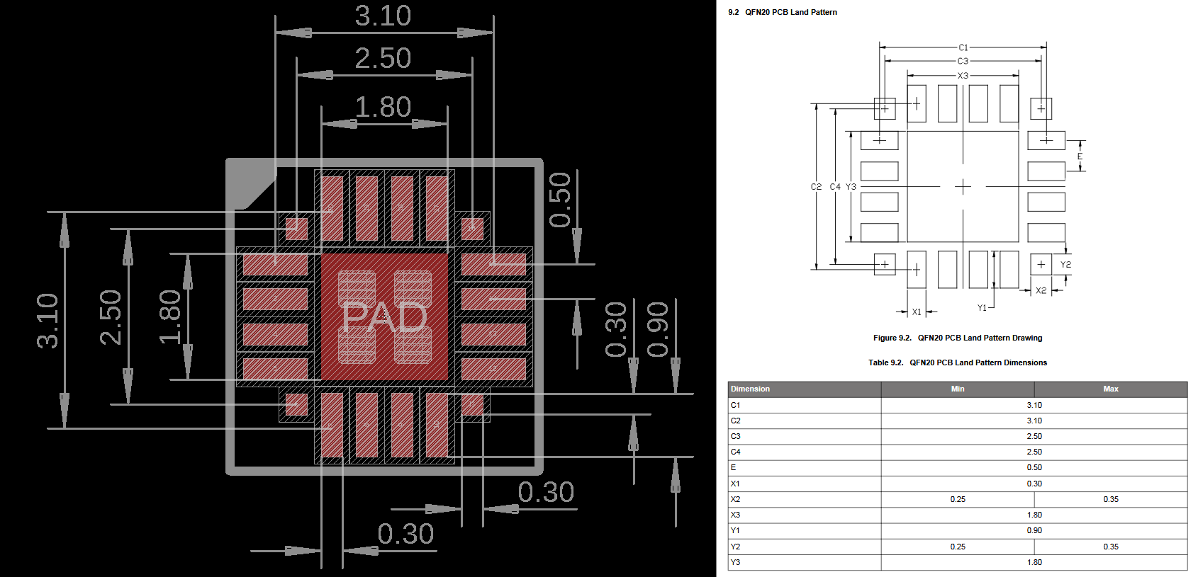
Figure 1. Silicon Labs EFM8UB10F8G in QFN20 package: comparison of the EDA tool layout with the datasheet landing pattern.
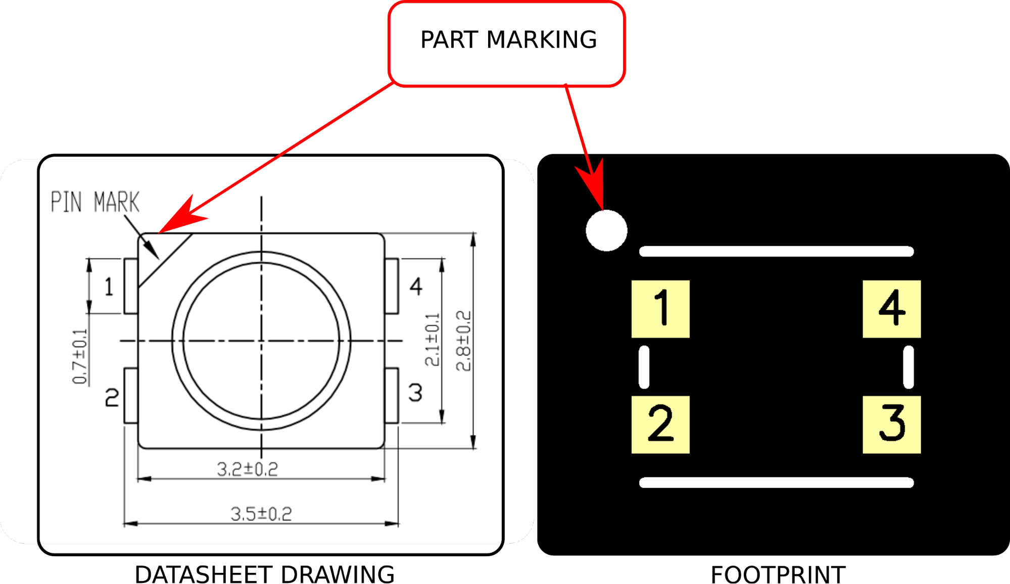
Figure 2. Pin‑1 marking on a CREE LED.
Build a Library of Tested Substitutions
Production can stall when a critical part becomes unavailable. Before you lock in a design, test any potential substitutes in a prototype. This reduces risk when you need to switch components later.
For unique parts that lack direct replacements, check the manufacturer’s end‑of‑life (EOL) status. Many vendors label EOL items as “Not Recommended for New Designs.” Ensure your chosen part remains available throughout the product’s lifespan to avoid costly redesigns.
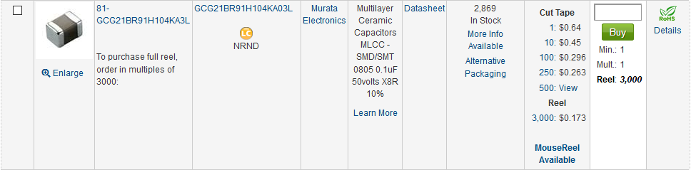
Figure 3. EOL marking on Mouser: NRND or Not Recommended for New Designs.
Leverage Pre‑Certified Radio Modules
Using a pre‑certified Bluetooth or Wi‑Fi module guarantees an FCC‑identified, compliant solution. These modules are pre‑designed, reducing the likelihood of radio‑emission failures during final testing.
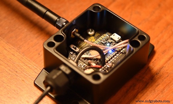
Figure 4. OSBeehives’ BuzzBox powered by a Particle Photon pre‑certified radio module.
Plan Your Wireless Antenna Layout Carefully
When integrating wireless transceivers directly on the PCB, follow the manufacturer’s recommended antenna layout. Matching impedance, selecting the right antenna, and tuning filters are all critical for optimal performance.
Pre‑compliance testing can surface frequency harmonics and other issues before you ship to the fab, saving time and money.
Include Decoupling Capacitors Near Every Active Pin
Stable voltage rails depend on properly placed decoupling capacitors. Place them as close as possible to each component’s power pins. For multi‑pin devices, add capacitors at every power pin, and consider grounding caps for sensors, ADCs, and FPGAs.
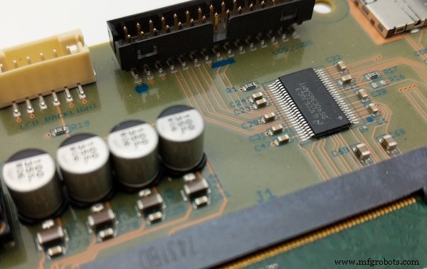
Figure 5. Decoupling capacitors ensuring smooth power to a Texas Instruments LVDS converter.
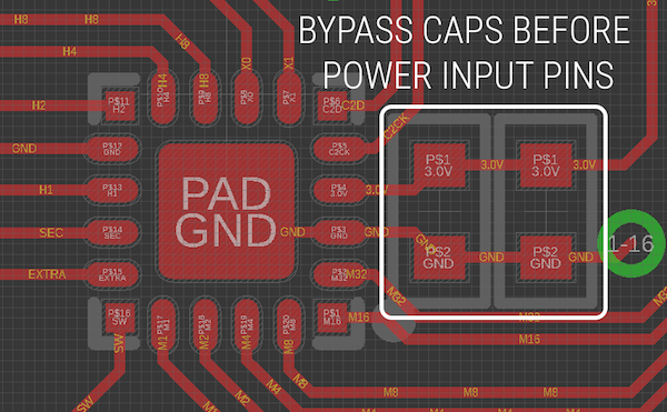
Figure 6. Bypass capacitors placed inline between the power source and the device.
Design for Adequate Trace Width and Spacing
High‑current traces must be sized to avoid overheating. Use an online trace‑width calculator, targeting a 10 °C temperature rise for internal traces and 20 °C for external traces. If the required width exceeds your board’s clearance, consider a thicker copper weight—just remember it may raise the cost and affect DRC spacing.
High‑voltage traces need sufficient isolation. When your board interfaces with mains voltage, ensure air gaps are large enough to prevent arcing.
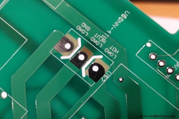
Figure 7. Routes cut out between pads for increased voltage isolation.
Choose the Right Regulator Layout
Linear Regulators
- Follow the manufacturer’s capacitor recommendations—place them as close to the regulator pins as possible.
- Manage heat: use copper pours and via stitching. If the pour is insufficient, add a heatsink.
Figure 8. Copper pours around a linear regulator to dissipate heat.
Switching Regulators
- Adhere strictly to the manufacturer’s layout guide—these are tested for reliability.
- Keep the feedback loop short to reduce EMF and parasitic effects.
- Check the output capacitor’s ESR and ESL ratings against the datasheet’s specifications.
Texas Instruments Webench can generate component recommendations and schematic snippets for a range of switching regulator designs.
Implement Thermal Relief for Large Pads
Thermal relief connects large copper pads to traces via narrow spokes, reducing the thermal load during soldering and preventing cold joints. Avoid making the relief too narrow to prevent current‑carrying failure.
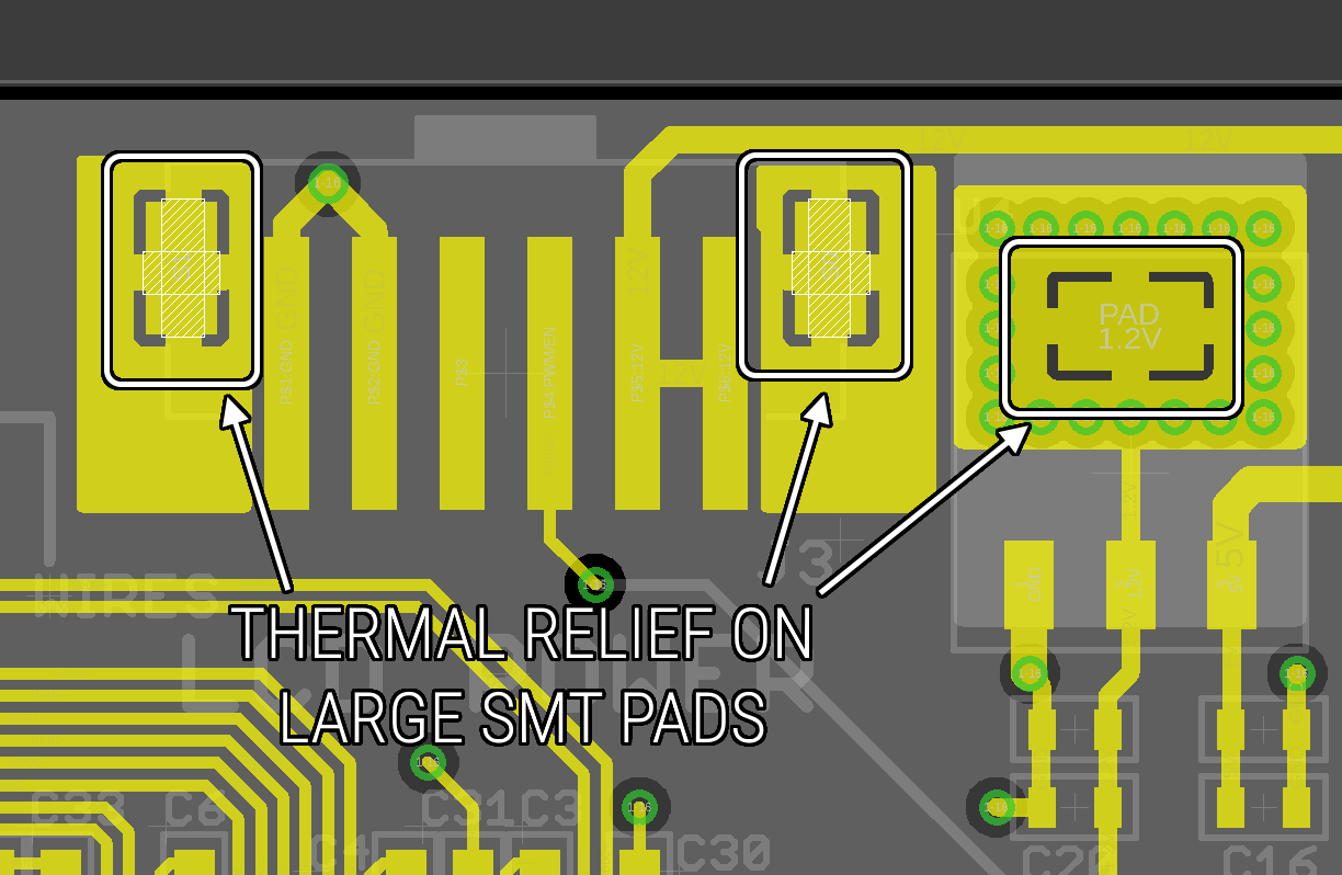
Figure 9. Thermal relief on a large SMT pad to promote proper soldering.
Optimize for SMT Assembly
Maximizing SMT components reduces both cost and assembly time. Use SMT connectors for parts that are only accessed during assembly, such as internal batteries. When through‑hole components are required—especially connectors that must be robust—coordinate with your contract manufacturer to allow sufficient clearance for wave or selective soldering.
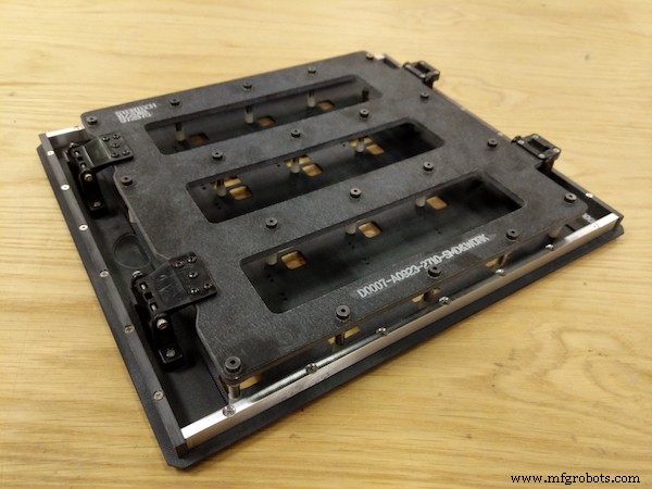
Figure 10. Wave pallet tooling enabling faster through‑hole connector soldering.
Verify Design Rule Checks (DRC) Thoroughly
Before sending Gerbers to your fab, run a final DRC and confirm:
- All clearance and width rules meet your manufacturer’s specifications.
- Signal routing is correct—use airwires or rat‑lines to trace net connections.
- Silkscreen text is up‑to‑date with date codes, PCB revisions, and other metadata.
Conclusion
By applying these PCB design best practices, you can reduce manufacturing risk, shorten time‑to‑market, and ensure regulatory compliance. For deeper insights, check out Parker’s interview with All About Circuits and his comprehensive pre‑FAB checklist.
Industry Articles are a form of content that allows industry partners to share useful news, messages, and technology with All About Circuits readers in a way editorial content is not well suited to. All Industry Articles are subject to strict editorial guidelines with the intention of offering readers useful news, technical expertise, or stories. The viewpoints and opinions expressed in Industry Articles are those of the partner and not necessarily those of All About Circuits or its writers.
Industrial Technology
- Cut CNC Machining Costs Without Compromising Quality
- 12 Expert Tips for Designing PCBs That Assemble Perfectly
- Mastering Rigid-Flex PCB Design: Expert Skills for Rapid, High-Quality Boards
- Microwave PCB Design: The Ultimate Solution for High‑Frequency Applications
- Mastering PCB Panelization: A Step‑by‑Step Guide to Efficient Assembly
- Essential Tips for Successful PCB Assembly
- Mastering Flawless PCB Assembly: Key Practices
- Mastering Design for Assembly (DFA): Key Principles & Best Practices
- Top 4 Strategies to Optimize Tolerances in Injection Molding
- Essential DFMA Guidelines for Efficient PCB Design & Production – Part I