


Why Wafer‑Level Chip‑Scale Packaging is Essential for Next‑Gen Wearable SRAMs
During a recent discussion on wearable technology, Ralph Osterhout, CEO of The Osterhout Design Group, noted, “What won’t work is a bulky device that distances people from their environment. If you’re talking about something that makes you look like a hammer‑head shark with wires? Then, no. It’s not going to work.” (source)
To keep board footprints low, microcontrollers continually move to smaller process nodes while adding more sophisticated functionality. This shift inevitably raises the need for larger on‑chip cache memory. Yet each new node makes integrating additional embedded SRAM more difficult due to higher soft‑error rates, lower yields, and increased power draw. Customers also demand highly customized SRAM options, making it impractical for MCU vendors to stock every possible cache size. Consequently, many designers opt to place the cache on an external SRAM chip.
But an external SRAM brings its own space penalty. With a six‑transistor cell layout, shrinking the SRAM die to a newer node still leaves a bulky package, and the same reliability and power issues that affect embedded SRAMs reappear.
One solution is to combine the SRAM die with the MCU die in a multi‑chip package (MCP) or 3‑D system‑in‑package (SiP). While this approach can reduce overall board area, it requires significant capital investment and limits post‑production flexibility. Replacing a single die in an SiP necessitates re‑qualification of the entire package, which is costly and time‑consuming.
Is there a way to keep the SRAM external yet drastically cut the package size? The answer lies in minimizing the die‑to‑package area ratio.
The most advanced method today is wafer‑level chip‑scale packaging (WLCSP). WLCSP assembles each die into a package immediately after dicing, eliminating bond wires or interposers. By design, a chip‑scale package occupies no more than 20 % larger area than the die, and modern processes can add only a thin layer of bump material, keeping the footprint virtually unchanged.
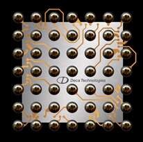
Figure. WLCSP, developed at Deca Technologies, preserves the die area while enabling high‑density packaging. (Source: Deca Technologies/Cypress Semiconductor)
Compared to a bare die, a CSP offers several advantages: easier testing and handling, lower assembly cost, and superior thermal conductivity. Moreover, when the die is fabricated in a newer process node, the CSP envelope can remain unchanged, allowing straightforward upgrades without redesigning the package.
For wearable and IoT applications, the volume savings are striking. A 48‑ball BGA SRAM typical of today measures 8 mm × 6 mm × 1 mm (48 mm³). In a WLCSP package, the same die fits in 3.7 mm × 3.8 mm × 0.5 mm, a reduction of roughly 85 % in volume. This shrinkage translates directly into smaller PCBs and thinner end‑products.
Consequently, the demand for WLCSP‑based SRAMs is growing beyond wearables into broader IoT ecosystems. Designers looking to leverage these benefits can consult resources such as “Getting Started with Chip‑Scale Packages” for best practices.
Embedded
- Why Mechanical Design Services Are Essential for Product Success
- Why Ultra‑Low, High‑Accuracy Pressure Sensors Are Critical for Modern Applications
- Cloud‑Enabled EDA: Accelerating Chip Innovation and Cost Efficiency
- SolarWinds Breach Shows Why Cybersecurity Must Be a Board‑Level Priority
- Designing an Electronic Spirit Level for the Visually Impaired
- Why Formal Maintenance Scheduling Is Essential for Efficient Operations
- Essential Gear for Successful Confined Space Rescues
- Why Open Source Drives Innovation at the Edge – Essential eBook
- Accurate Hydraulic Fitting Measurement: Step‑by‑Step Guide
- Hydraulic Systems: Why Regular Maintenance Is Essential