


Samsung Unveils H‑Cube 2.5D Packaging, Supporting 6‑HBM Integration for HPC & AI
Samsung Electronics has unveiled the H‑Cube hybrid‑substrate technology—a 2.5D packaging platform engineered for high‑performance semiconductors in HPC, AI, data‑center, and networking applications that demand extensive area and superior performance.
Co‑developed by Samsung Electro‑Mechanics (SEMCO) and Amkor Technology, H‑Cube addresses the need for large‑scale integration of silicon dies. Samsung states that the new package expands the foundry ecosystem, offering a breadth of solutions to meet customers’ evolving demands.
“In today’s environment where system integration is increasingly required and substrate supplies are constrained, Samsung Foundry and Amkor Technology have successfully co‑developed H‑Cube to overcome these challenges,” said JinYoung Kim, senior vice president of global R&D at Amkor Technology. “This development lowers barriers to entry in the HPC/AI market and demonstrates successful collaboration and partnership between the foundry and outsourced semiconductor assembly and test (OSAT) company.”
H‑Cube structure and features2.5D packaging places logic chips or high‑bandwidth memory (HBM) on top of a silicon interposer in a compact footprint. Samsung’s H‑Cube combines a fine‑pitch interposer capable of fine‑bump connections with a high‑density interconnect (HDI) substrate, enabling large‑scale 2.5D packages.
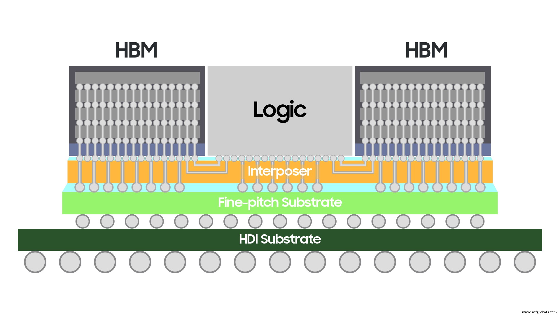
As HPC, AI, and networking workloads push higher specifications, large‑area packaging becomes essential when the number and size of chips per package grow or when high‑bandwidth interconnects are required. Fine‑pitch substrates are indispensable for attaching silicon dies, but their cost escalates sharply with increased area.
When integrating six or more HBMs, manufacturing large‑area substrates becomes increasingly challenging, reducing yield and efficiency. Samsung tackled this by adopting a hybrid substrate architecture that layers an easily scalable HDI base beneath a high‑end fine‑pitch interposer.
By reducing the solder‑ball pitch by 35% compared to conventional ball pitch, the fine‑pitch substrate footprint shrinks, while the underlying HDI layer guarantees robust connectivity to the system board.
To further bolster reliability, Samsung applied its proprietary signal‑ and power‑integrity analysis, ensuring stable power delivery and minimizing signal loss or distortion when stacking multiple logic chips and HBMs.
Embedded
- Industrial Technology: A New Era of Efficiency and Growth
- ACEO® Unveils Breakthrough Silicone 3D Printing Technology
- Desktop Metal’s BMD and Microwave Sintering: A New Era for Metal Additive Manufacturing
- Smart Technology Solutions for Social Distancing in Retail
- DATA MODUL Launches Hybrid Bonding Technology for High‑Volume Industrial Touch Displays
- BASF Supplies Advanced Additive Materials to Paxis for WAV 3D Printing Innovation
- INOMETA Expands Portfolio with Advanced Laser‑Assisted Tape Winding System
- OnRobot Launches 2FG7: Cleanroom‑Ready, IP67‑Certified Parallel Gripper for Rapid, Cost‑Effective Automation
- Avnet Silica Launches MiniPOC Kit: Accelerating Industrial IoT Edge‑to‑Cloud Proof‑of‑Concepts
- Universal Robots Launches Advanced Interface for e-Series Cobots in Injection Molding