


Scanning Electron Microscopy (SEM): Unveiling Materials Defects with Advanced Imaging
Do you know what electron microscopy is and what is it capable of analyzing? The ATRIA materials team explains it to you in this post!
Many of the defects that occur in materials are difficult to explain and defining their causes can be a very complex task. However, today the great advances in microscopic analysis technology are at our fingertips, which can provide us with key information to find the explanation for the origin of the failure.
What is Scanning Electron Microscopy or SEM?
Electron microscopy is based on the emission of a scanning beam of electrons on the sample, which interact with it, producing different types of signals that are collected by detectors. Finally, the information obtained in the detectors is transformed to give rise to a high definition image, with a resolution of 0.4 to 20 nanometers. In conclusion, we obtain a high resolution image of the surface topography of our sample.
With it we can study different types of materials (below you can see that their preparation is not the same in all cases):
- Metals: steel, aluminum, titanium, copper, precious metals, alloys, …
- Ceramics: glass, concrete, alumina, zirconia, carbide, stone, porcelain …
- Polimers: thermoplastics like PP, PE, Nylon; thermosets such as melamine, polyimides; elastomers such as rubber, silicone, …
- Composites: carbon fiber, fiberglass, graphite, ceramic composites, resins, …
- Organics: cotton, wood, bacteria, cells, …
How does Scanning Electron Microscopy (SEM) works?
Scanning electron microscopes (SEM) have a filament that generates a beam of electrons that impact the sample. These electrons interact with the sample that is being studied and return different signals that are interpreted by different detectors. With this information we are able to obtain superficial information from:
-
Shape and topography
-
Texture
-
Composition
The interaction of the electron beam with the surface of the sample takes place in a ‘pear’ shape as you can see in the image below. The penetration will depend on the kV at which we work, a standard is a penetration of 1-5 microns.
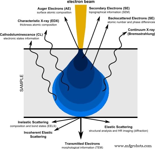
Electron beam interaction with the sample, ‘pear’ model
Detectors in a scanning electron microscope (SEM)
The most common detectors are the following:
-
Secondary Electron Detector (SE): captures the energy from the secondary electrons generated in the material by the interaction of the electron beam. They provide the information on the most superficial texture / topography as it comes from the outermost layer (the ‘pear’ closest to the surface in the lower image).
-
Backscattered electron detector (BSE): it captures the energy coming from the backscattered electrons (second layer of the ‘pear’). It has less surface resolution but is sensitive to variations in the atomic number of surface elements, and therefore in composition. We will observe a different shade of gray according to the atomic weight (clearer if the element is heavier since it emits more energy and ‘shines’ more).
-
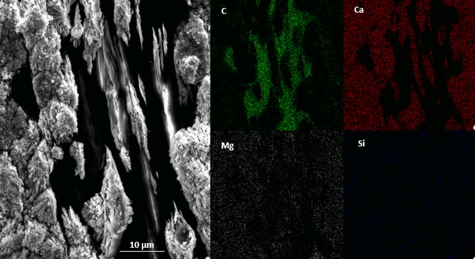
X-ray detector (EDX, EDS or EDAX): this detector captures the energy from the X-rays generated on the surface (third layer of the ‘pear’) and they are characteristic of each element of the sample so they provide us with information about elemental composition. Unlike the BSE, they provide us with more information on the sample. allows us to know in a semi-quantitative way the composition of the surface of our sample. EDXs can be applied to a specific point on the sample surface or to an area. When the analysis is applied to an area, it is possible to obtain a map with the different elements that the selected area of the sample has, each element being represented with a different color. You can see it in the image of one of our Projects below.
-
X-ray Detector (WDS): similar to EDX, but instead of receiving the energy of all X-rays at once, it only measures the signal generated by a single element. It is a slower but more sensitive and precise technique.
-
Diffracted backscattered electron detector (BSED): this detector receives the energy of electrons diffracted by the surface that comply with Bragg’s law and provide information on the crystal structure of the sample.
Left. SE Detector; Right. BSE Detector
EDX with FEI microscopio
Types of scanning electron microscopy according to source
You may have seen terms like SEM, FE-SEM or FIB-SEM, do you know their differences? go for it!:
-
SEM: these are the conventional SEMs that we have already explained and have a thermal source of electrons.
-
FE-SEM (field emission SEMs): they are the evolution and have as an electron source a field emission gun to provide the high and low energy electron beams. As these beams are very focused, they allow better resolution.
-
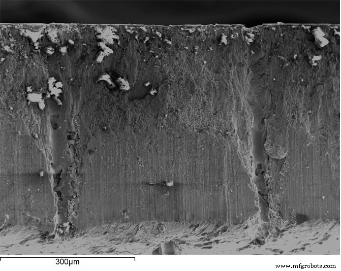
Dual Beam o FIB-SEM (double beam microscope or focused ion beam SEMs): it has two columns, one of ions and the other at 52º of electrons. The ion column uses a Gallium (Ga +) ion beam. Ga + ions are 130,000 heavier than electrons, so the interaction with the sample is stronger although its penetration is less. Additionally, ion slices can be made to visualize the inner layers.
Dual Beam image in which an ion cut was performed
Types of scanning electron microscopy according to vacuum
Depending on the type of vacuum there are several types of SEM:
-
High vacuum SEM: the sample needs to be dry and conductive. For non-conductive samples, these can be coated with a carbon or metal sputtering layer.
-
No vacío o environmental SEM (ESEM): no se necesita preparación de muestra. SE pueden analizar muestras biológicas y no conductoras sin necesidad de recubrir.
Differences between an optical microscope (OM) and a scanning electron microscope (SEM)
We tell you the main differences between an optical microscope and a scanning electron microscope:
-
Increases: optical microscopes can have from 4x to about 1000x, while SEM can range from 10x to more than 3,000,000x.
-
Field depth: or what is the same, how much sample is focused at the same time. In the case of optical microscopes, they range from 0.19 microns to 15 microns. In SEMs, this range is broader, ranging from 0.4 microns to 4 mm.
-
Resolution: optical microscopes can reach a spatial resolution of about 0.2 microns, while SEMs can reach up to 0.4 nm with some models and lenses.
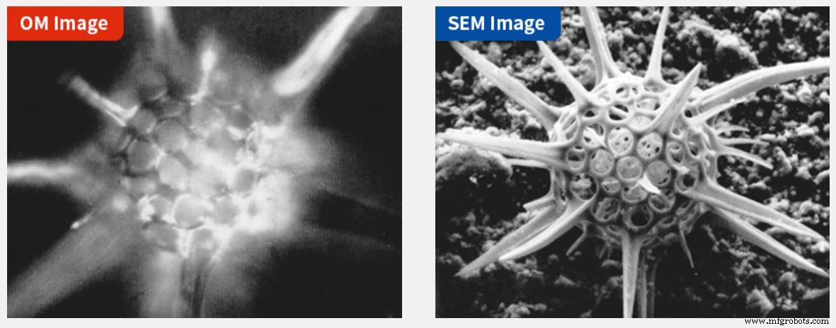
Left Image with optical microscope; Right SEM image with Nanoimages microscope.
Advantages of electron microscopy compared to other characterization techniques
Electron microscopy is a very useful technique in the characterization of materials since very little amount of sample is needed and it is a non-destructive technique (as long as the sample does not have to be cut to fit on the slide or coat), that is, , the sample is not damaged and can be recovered. The only requirement that the use of this technology implies is that the sample must be conductive, since obtaining the image is the product of the interaction of the electrons emitted by the equipment and the sample. If our sample is not conductive, there is no problem, as we have already seen, since they can use sample metallizers that deposit a few nanometer layer of a conductive element by means of physical vapor deposition, thus allowing the obtaining of Composition and scanning electron microscopy images through EDX. The images obtained have a high resolution.
Both the purely imaging part and its EDX detector are non-destructive and fast response techniques, which is why they are considered powerful tools in the characterization of all types of materials, since they allow us to know what type of surface topology our sample has, its defects and its composition with the obtaining of a single image.
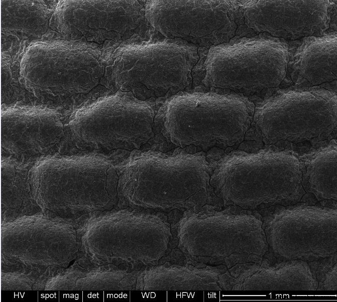
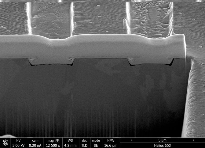
Microperforations manufactured by laser and observed by FESEM
SEM Scanning Electron Microscopy Applications
At ATRIA, electron microscopy is a widely used and well-known tool. These types of techniques are used in different sectors such as automotive, construction, consumer goods, retail, defense, dentistry or packaging, among others.
Electron microscopy can be used for applications as varied as:
-
Product design failure analysis: to know why a failure has occurred, for example in this Project the morphology and composition of defects that appeared in the quality tests of a product were characterized. Another type of failure that can be studied are: delaminations, adhesion, …
-
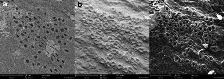
Characterization of surface texturing: when the topography and structure that has been generated wants to be known, for example, with samples through laser technology, the SEM is a very useful tool, in this Project it also allowed the optimization of the laser parameters of marked.
-
Analysis of surface defects and quality control: by means of the SEM it is possible to visualize the defects, to know the typology, for example in this Project we study the defects that appear under the normal behavior of use of the products.
-
Study of contaminants: thanks to the EDX detector it is possible to find unwanted contaminants in the samples, which cause adhesion problems, painting or structural failures. You can see an example of a Project that we have carried out on the study of contaminants in paints with which we saw key differences through EDX.
-
Morphological and structural study: it involves the identification and analysis of crystalline phases and transitions in different materials such as metals, polymers, ceramics, minerals or composites. Thanks to the SEM it is possible to study the type of degradation such as fatigue, corrosion, cracks, …
-
Competitor analysis: the SEM technique is also used to study competitive products and perform benchmarking.
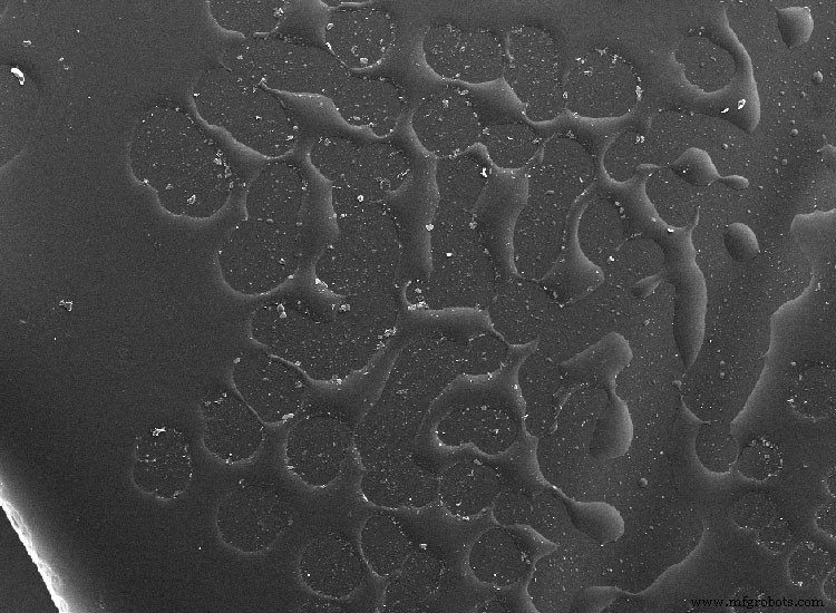
SEM image in which we can see the surface contamination as brighter points that should not appear so there is a poor adhesion of the paint
Do you need to analyse the microstructure of the surface of your product? Would you like to investigate those products that turn out to be defective? Does a defect appear continuously, and would you like to know what it is due to? Tell us about it on our networks, write to us at info@atriainnovation.com or fill out our contact form.
Related posts:
What are quality tests and product tests
Hydrophobicity of materials
Microstructuring by laser pattern interference
IN-MOLD MICROSTRUCTURATION to improve the cleaning properties of injected plastics
Related projects:
Irreversible stains study on synthetic fabrics
Hydrophilic microstructures development
Metallic paint reticulation analysis
Composite material
- Key Applications of Hafnium: From Nuclear Control Rods to Advanced Alloys
- Master C++ For Loops: A Step-by-Step Guide
- Master Java For Loops: Syntax, Examples, and Best Practices
- What is Quantum Computing? A Beginner’s Guide
- Thermography Explained: How Infrared Imaging Detects Temperature Variations
- Shape Memory Materials: How They Bend, Rebound, and Transform Under Heat
- Explore the Versatile Applications of 3D Printing in Industry and Healthcare
- Naval Brass: Superior Strength & Corrosion Resistance for Industrial Use
- A286 Alloy Explained: Composition, Applications, and Benefits
- Key Criteria for Selecting a Trusted Metal Supplier