


IBM Breakthroughs in 7nm BEOL Technology: EUV Lithography and Cobalt Metallization Propel Next‑Gen Chips
Dr. Griselda Bonilla serves as Senior Manager of IBM Research’s Advanced BEOL Interconnect Technology team, steering breakthroughs that elevate the company’s industry‑leading on‑chip interconnect (BEOL) solutions. We spoke with her prior to her team’s presentations at the IITC/AMC Conference in San Jose, California, this week.
First off, tell us a bit about why 7nm technology is such a big deal.
Griselda Bonilla: The 7 nm node is a linchpin for next‑generation systems—cloud, big data, cognitive computing, and mobile. Following a $3 billion investment in 2014 and collaborations with New York State, GLOBALFOUNDRIES, and Samsung, our innovations in materials, tools, and processes could deliver up to a 50 % boost in power‑performance for these platforms. Achieving the 7 nm milestone through new materials and EUV lithography is a strong indicator of this potential.
What was your role in last year’s breakthrough 7nm node test chip?
GB: I managed a large, cross‑functional team that defined and developed a new, reliable interconnect technology at a 36 nm pitch.
What has the progress been like since last year’s breakthrough?
GB: The journey has been exhilarating. BEOL scaling remains a formidable challenge for modern CMOS nodes, including the 7 nm node we’re pushing. Our focus has been on back‑end‑of‑line interconnects that link transistors, capacitors, resistors, and more. The copper wiring we’re working with is now less than 1/20th the size of the original Cu interconnects introduced nearly two decades ago. For the first time, we’ve demonstrated aggressively scaled interconnects using extreme ultraviolet (EUV) lithography, offering unprecedented flexibility in circuit design—a critical advantage as other patterning techniques grow increasingly complex and restrictive.
Tell us about the IITC/AMC Conference. What are you presenting, and why is this the place to introduce your work?
GB: The IITC/AMC Conference is the premier gathering for BEOL research, bringing together industry leaders and academics to exchange the latest advances. We were invited to deliver two talks: "7 nm BEOL Technology" and "BEOL Design Technology Co‑Optimization for Beyond 7 nm Technology." My colleague, Dr. Theo Standaert, leads the team that authored our 7 nm BEOL technology paper and is responsible for defining and validating interconnect solutions for future nodes. In addition, we presented six contributed talks and four posters covering key BEOL performance metrics, novel integration methods, and materials. IBM Research Alliance secured the most papers and talks at this year’s conference.
Tell us more about the Alliance. How have GLOBALFOUNDRIES, SUNY Polytechnic Institute, and the other partners contributed?
GB: These collaborations are foundational. They enable exploration of cutting‑edge BEOL innovations through a unique blend of IBM’s deep research expertise, GLOBALFOUNDRIES’ and Samsung’s manufacturing prowess, and SUNY Poly’s academic innovation and leadership.
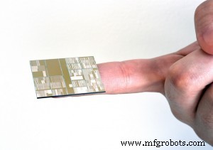
Close‑up of IBM 7 nm node test chip produced at SUNY Poly CNSE in Albany, NY. (Darryl Bautista/Feature Photo Service for IBM)
SiGe channel material and EUV lithography were pinpointed as breakthroughs last year. What are the new complementary materials or techniques being employed now?
GB: We are spotlighting cobalt metallization at the contact level, alongside the technical innovations required to achieve a reliable BEOL interconnect at these aggressive dimensions.
What do these advancements mean in terms of being able to mass produce a 7nm chip?
GB: They enable interconnect scaling to continue into the 7 nm node with proven yield and reliability. We’ll present an industry‑first, full evaluation of breakthrough contact/local interconnect metallurgies, targeting a 2.5‑fold reduction in contact resistance—critical for overcoming the severe performance bottleneck posed by high resistance in 10 nm and 7 nm CMOS ULSI.
What is the significance of the local interconnects breakthrough?
GB: This marks the first change to contact metallurgy since the inception of damascene processing—an additive technique that creates Cu interconnects—almost 25 years ago. This advancement is pivotal for 7 nm technology, offering a tangible path to mitigate performance loss associated with traditional tungsten contacts.
Nanomaterials
- Digital Maintenance: Winning the Race Against Aging Equipment
- Tiny 3D Image Sensor Uses Time‑of‑Flight Technology
- Last Chance to Register for PT Tech Days – Expert Sessions on Injection Molding & Extrusion
- Revolutionizing Mobile Connectivity with eSIM: NetLync’s Vision
- Five Industries Poised for Technological Disruption in 2024
- Upgrade Mobile Tech in Transportation: Unlock Efficiency & Growth
- How Emerging Technologies Are Reshaping Modern Workplaces
- MT360: Bridging Manufacturing and Tech Communities
- Paper Tab: Revolutionizing Tablets with Flexible Paper Technology
- Upgrade Your Factory: Why Now Is the Best Time to Invest in New Manufacturing Tech