


Quantum Devices: Beyond CMOS – Harnessing Tunneling, Quantum Dots, and Spintronics for Future Electronics
Since the 1960s, CMOS technology has followed a predictable scaling trajectory: gate lengths have shrunk from the micron scale to the 65‑nm nodes now in production, with 45‑nm transistors expected by 2007. At 65‑nm, leakage currents driven by quantum tunneling begin to dominate, and at 45‑nm, sophisticated engineering is required to suppress this leakage. The conventional scaling limit for MOS transistors is projected to lie between 20‑ and 30‑nm, with some experts citing 1‑ to 2‑nm as the ultimate physical boundary. Photolithography will continue to improve, yet sub‑20‑nm devices demand new active structures that exploit, rather than fight, quantum mechanical effects.
When MOS geometries approach the electron’s de Broglie wavelength, tunneling through the gate oxide and the narrow channel becomes significant. This quantum leakage forces the industry to explore devices that leverage tunneling for performance and energy efficiency. Key candidates include resonant tunneling diodes (RTDs), double‑layer tunneling transistors (Deltt), metal‑insulator‑insulator‑metal (MIIM) diodes, quantum dot transistors, and graphene‑based devices. Spin‑based electronics (spintronics) also offer a non‑dissipative alternative to charge‑controlled logic.
Quantum Tunneling
Quantum tunneling: An electron behaves as a wave that can pass through an insulating barrier thinner than its wavelength, enabling a probability of transmission even when classical physics predicts reflection.
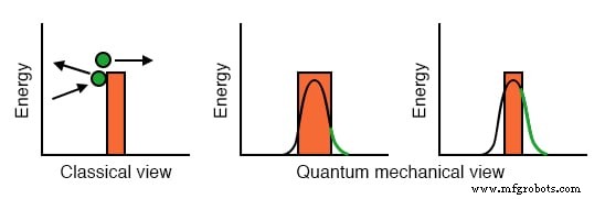
Classically, an electron must possess enough energy to surmount a barrier; otherwise it reflects. Quantum mechanics allows a non‑zero probability of finding the electron on the far side of a sufficiently thin barrier. The tunneling probability increases sharply as the barrier thickness decreases.
Tunnel Diode
Tunnel diode: The Esaki tunnel diode is an early quantum device that relies on a heavily doped depletion region—about 1,000 times the doping level of a standard rectifier—making the barrier thin enough for tunneling when appropriately biased.
Resonant Tunneling Diode (RTD)
RTD: An RTD is a quantum device featuring two tunneling barriers separated by a quantum well. Electrons traverse the device when the source energy aligns with a quantized level in the well, a condition known as resonance. The current rises as the bias approaches resonance, then falls when the energies misalign again, enabling a natural on/off behavior that can replace pairs of conventional transistors in logic cells.
RTDs have demonstrated oscillation frequencies up to 712 GHz. Their on/off switching makes them attractive for reducing component count, area, and power consumption compared to traditional CMOS circuits. [GEP] [ERB]
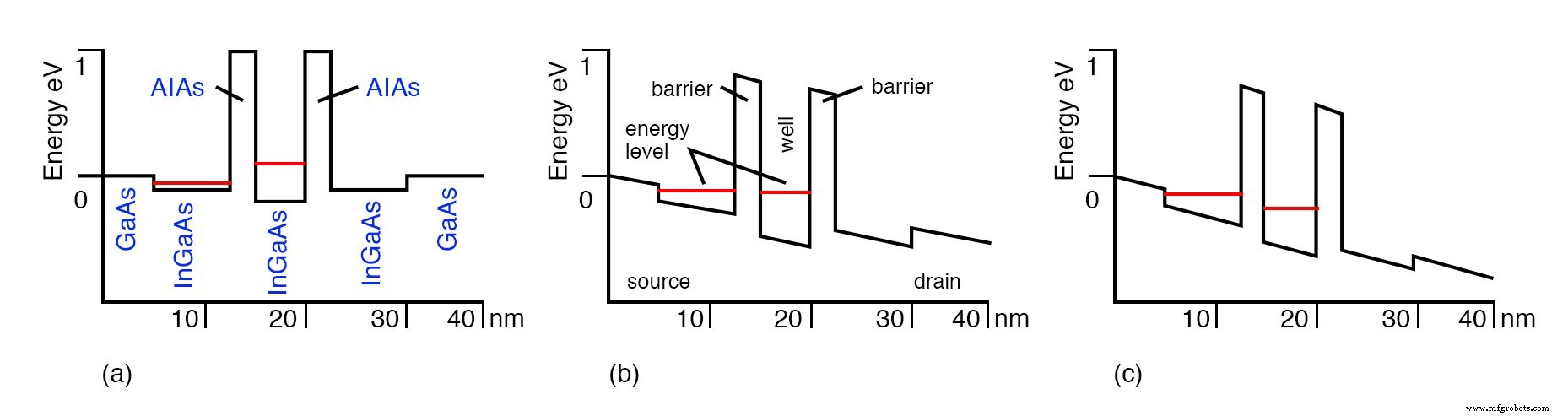
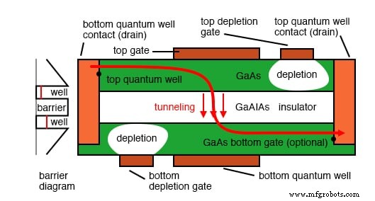
Double‑Layer Tunneling Transistor (Deltt)
Deltt: The Deltt consists of two ultrathin conductive wells (quantum wells) separated by a high‑band‑gap insulator such as GaAlAs. When the gate voltages align the energy levels of the two wells, electrons tunnel through the barrier, turning the device on. Excessive bias misaligns the levels, turning it off. The device behaves like a complementary pair without requiring separate p‑ and n‑type transistors, and operates on a ~100 mV supply.
Deltt prototypes have functioned at 4.2 K, 77 K, and 0 °C; room‑temperature operation is anticipated. [GEP] [IGB] [PFS]
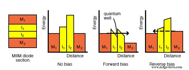
Metal‑Insulator‑Insulator‑Metal (MIIM)
MIIM diode: A quantum tunneling device that uses two insulating layers between metal electrodes. The insulators must be thinner than the electron’s de Broglie wavelength. Under forward bias, a quantum well forms between the insulators, dramatically increasing tunneling probability and producing a sharp forward characteristic. MIIM diodes outperform conventional MIM diodes in frequency response, reaching 3.7 THz. Adding a third electrode converts the structure into a transistor. [PHI]
Quantum Dot Transistor
A quantum dot—an isolated nanoscale conductor—can store discrete charges, with a 1‑ to 3‑nm dot holding a single electron. When such a dot is placed over a thin insulator and coupled to a gate, the gate voltage can align the dot’s energy level with the source, enabling a single electron to tunnel onto the dot (the “single‑electron box”). Embedding the dot between source and drain turns the dot’s charge state into a gate‑controlled modulation of the source‑to‑drain current, analogous to an RTD or Deltt. This approach allows a single transistor type to form complementary logic. [GEP]
Single Electron Transistor
When two tunnel barriers surround a tiny conductive island, the addition of a single electron changes the island’s potential so dramatically that further tunneling is blocked—a phenomenon called Coulomb blockade. This mechanism underpins single‑electron transistors, which typically require cryogenic temperatures. Graphene‑based islands, however, have demonstrated room‑temperature operation. [GEP]
Graphene and Carbon Nanotube Transistors
Graphene transistor: Graphene, a single‑atom‑thick sheet of carbon, exhibits exceptional conductivity without doping. Fabricated transistors using graphene gates show low power dissipation and high switching speeds, positioning graphene as a potential silicon replacement. Graphene quantum dots enable single‑electron transistor behavior at room temperature. [AKG] [JWA]
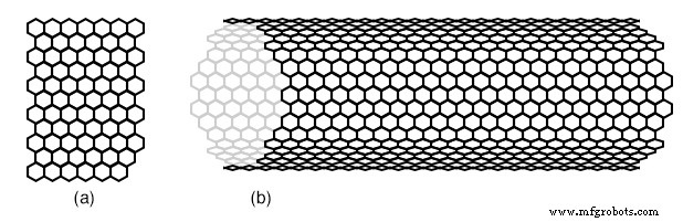
Carbon nanotube transistor: Rolling a graphene sheet into a tube yields a 1‑dimensional conductor that supports ballistic transport, minimizing scattering. Both metallic and semiconducting nanotubes have been integrated into field‑effect transistors, offering smaller, faster, and lower‑power alternatives to silicon. [MBR] [PNG]
Spintronics
Spintronics exploits the electron’s spin—up or down—as a binary state, enabling data storage and logic with minimal energy dissipation. Magnetic tunnel junctions (MTJs) consist of two ferromagnetic layers separated by a thin insulator; the junction’s resistance depends on the relative spin alignment. Adding an antiferromagnetic pinning layer stabilizes the reference magnetization, enhancing read/write sensitivity. MTJ arrays embedded in silicon wafers provide non‑volatile, high‑speed memory that already exists in commercial products. [WJG] [IBM] [TLE]
Future spin transistors, though not yet realized, could enable logic gates that propagate spin without charge movement, dramatically reducing power usage. Spin injection via ferromagnetic contacts or circularly polarized light has been demonstrated, opening pathways to spin‑based electronics. [DDA] [RCJ2]
REVIEW:
- Gate‑oxide thinning in MOS transistors causes unacceptable leakage and heating, marking the practical limit of conventional scaling.
- Resonant tunneling diodes use quantum tunneling to achieve high‑speed, low‑power amplification.
- Deltt transistors control tunneling between quantum wells, enabling complementary logic without separate p‑ and n‑devices.
- Quantum dot transistors replace the gate with a single‑electron island, modulating current through Coulomb blockade.
- Spintronics manipulates electron spin rather than charge, offering non‑dissipative data processing.
RELATED WORKSHEETS:
- Electrical Conduction in Semiconductors Worksheet
Industrial Technology
- Active vs. Passive Electronic Components: Understanding Their Roles
- Quantum Physics and the Atom: Foundations for Modern Electronics
- Superconducting Devices: Fundamentals, Applications, and Emerging High‑Temperature Technologies
- Comprehensive Guide to Semiconductor Device Modeling in SPICE
- IoT Security: Overcoming Deployment Barriers
- Revolutionizing Industry: The Future of Connected Devices
- Protecting IoMT: Best Practices for Securing Internet-Connected Medical Devices
- Protecting Your Data: The Ultimate Guide to IoT Privacy & Security
- Windlass Safety Devices: Essential Protective Features for Marine Operations
- Generator Protection: Fault Types & Essential Protective Devices