


Understanding Depletion‑Type IGFETs: Design, Operation, and SPICE Analysis
Insulated gate field‑effect transistors (IGFETs) are unipolar devices, much like JFETs: the controlled current flows entirely within a single type of semiconductor, so no PN junction is crossed by the current.
Inside the device, a PN junction exists solely to form the non‑conducting depletion region that limits current through the channel. The junction itself never carries current.
Schematic Symbol and Physical Diagram
Below is a schematic of a depletion‑type N‑channel IGFET:
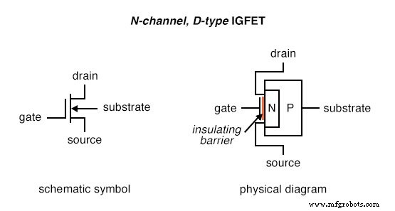
Notice how the source and drain leads attach to either end of the N‑channel, while the gate connects to a metal plate separated by a thin insulating barrier—commonly silicon dioxide, the main component of sand. This Metal‑Oxide‑Semiconductor (MOS) construction is why many IGFETs are also called MOSFETs, though “IGFET” better describes the entire class of insulated‑gate devices.
Modern IGFETs usually tie the substrate to the source internally, yielding a three‑terminal device. The schematic below reflects that common configuration:
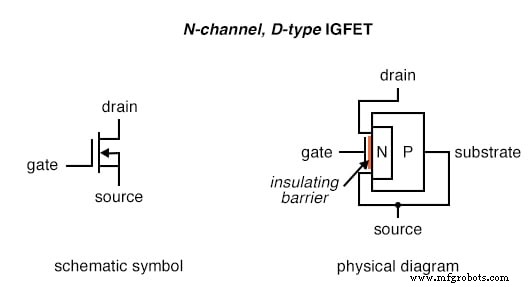
Because the substrate and source are electrically common, no voltage can be applied across the internal PN junction. Consequently, the depletion region cannot be expanded or collapsed as in a JFET; instead, the IGFET’s operation hinges on the displacement of that depletion region relative to the gate.
N‑channel IGFET
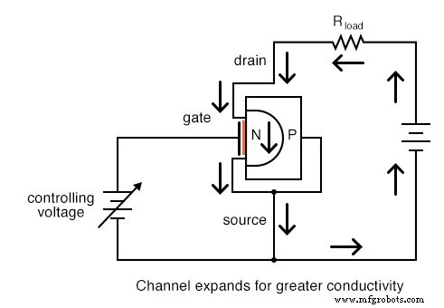
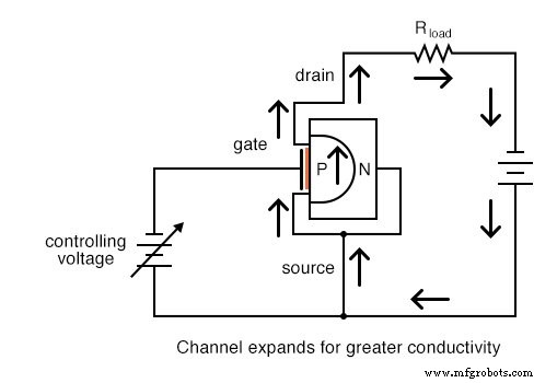
Applying a positive voltage to the gate relative to the source repels the depletion region, widening the N‑type channel and increasing conductivity:
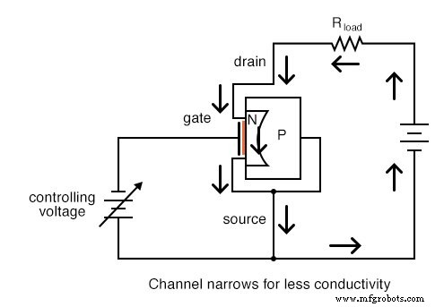
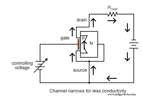
Reversing the polarity attracts the depletion region, narrowing the channel and reducing conductivity:
The insulated gate permits any polarity of controlling voltage without risking forward bias of the internal junction—a concern that limits JFETs. Although labeled a “depletion‑type,” the device can be either depleted (channel narrowed) or enhanced (channel expanded) depending on the gate‑to‑source voltage polarity.
To predict the effect, match the semiconductor doping of the channel (N‑ or P‑type) with the sign of the source voltage. For an N‑channel device, a positive gate and negative source enhance the channel by accumulating electrons on the channel side of the dielectric. If the polarities are swapped, electrons are removed from the channel, depleting it and lowering conductivity.
P‑channel IGFET
P‑channel devices obey the same principle, but the required polarity is reversed. The following images illustrate the biasing:
With zero gate‑to‑source voltage, a depletion‑type IGFET conducts between source and drain, but not at full capacity—unlike bipolar transistors, which are normally off, or JFETs, which are normally on. In effect, it behaves as a half‑on device.
Because the gate is insulated, the IGFET tolerates gate‑source voltages of any polarity. The PN junction is protected, and the direct source‑substrate connection prevents any voltage differential across the junction.
Remarkably, the conduction behavior of a D‑type IGFET resembles that of early vacuum tubes, where the grid voltage could either suppress or enhance the flow of electrons between cathode and anode.
SPICE Simulation of D‑type IGFET
The following SPICE runs illustrate the current‑regulating nature of a depletion‑type IGFET.
First, with the gate shorted to the source (0 V) and the supply swept from 0 V to 50 V, the drain current settles at a regulated 10 µA over the entire range:
n-channel igfet characteristic curve m1 1 0 0 0 mod1 vammeter 2 1 dc 0 v1 2 0 .model mod1 nmos vto=-1 .dc v1 0 50 2 .plot dc i(vammeter) .end
Applying a negative gate voltage of –0.5 V while sweeping the supply again reduces the regulated drain current to 2.5 µA:
n-channel igfet characteristic curve m1 1 3 0 0 mod1 vin 0 3 dc 0.5 vammeter 2 1 dc 0 v1 2 0 .model mod1 nmos vto=-1 .dc v1 0 50 2 .plot dc i(vammeter) .end
Conversely, a positive gate voltage of +0.5 V increases the current to 22.5 µA:
n-channel igfet characteristic curve m1 1 3 0 0 mod1 vin 3 0 dc 0.5 vammeter 2 1 dc 0 v1 2 0 .model mod1 nmos vto=-1 .dc v1 0 50 2 .plot dc i(vammeter) .end
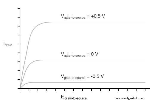
These results confirm the nonlinear relationship between gate‑to‑source voltage and drain current, analogous to that seen in JFETs. A depleting voltage of about –1 V can pinch off the channel, reducing the drain current to virtually zero. The exact pinch‑off voltage varies with each device’s specifications.
Characteristic Curve of IGFET
Plotting multiple characteristic curves for different gate voltages yields a pattern similar to a JFET’s family of curves:
RELATED WORKSHEET:
- Insulated Gate Field‑Effect Transistors Worksheet
Industrial Technology
- Hybrid Transistor Design: IGFET‑BJT Combo for High Gain and Low Drop
- Enhancement‑Mode IGFETs: Fundamentals, Applications, and Design Considerations
- Understanding Active-Mode Operation in IGFETs: Design, Performance, and Applications
- Common‑Source Amplifier (IGFET): Design, Biasing, and Performance
- Common‑Drain Amplifier (IGFET): Design, Function, and Applications
- Common‑Gate IGFET Amplifier: Theory, Design, and Practical Applications
- Expert Guide to Biasing Techniques for IGFETs
- Choosing the Right Transistor Ratings and Packages for IGFETs
- Common IGFET Quirks & How to Mitigate Them
- Mastering LED Strip Channels: Your Comprehensive Guide