


EMC PCBs: Reliable Solutions to Mitigate Electromagnetic Interference
Have you encountered a TV interfere with radio signals before? Or have you ever wondered why you switch off electronic devices when boarding a plane? Well, the reason is simple; electromagnetic interference (EMI).EMI is a pretty common phenomenon with electronic devices. But the question here is: How do you control EMI? That’s where the EMC PCB steps in. While you can’t eliminate EMI, you can reduce its effect and prevent interference with this PCB design.
Read on to learn more about EMC PCBs and how to design them.
What is EMI/EMC in PCB?
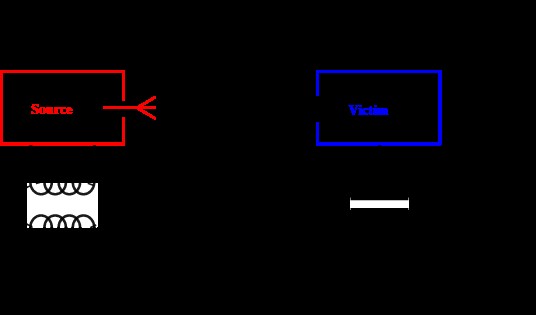
Electromagnetic Interference
EMI is like a disease that affects electronic circuits. Indeed, it’s an electronic disturbance that corrupts the signal quality of any electronic circuit and causes malfunctions. Also, this electronic disturbance is energy that travels through conduction or radiation from electronic devices.
Interestingly, EMI can affect the device creating a disturbance and other devices in close range. Electromagnetic interference can happen at any frequency but usually starts beyond 50MHz.

Electronic Devices
On the other hand, EMC (Electromagnetic compatibility) enables electronic systems to work without releasing heavy EMI. It also allows a system to determine optimal performance when working under safe conditions.
All electronic devices you build must not deviate from the EMI/EMC standards. Otherwise, EMI will continuously affect performance. Hence, you must control EMI while designing your PCBs.
Plus, it’s not easy to control EMI after completing your designs. So, in truth, you will spend a lot of money, which might not fix the problem.
So, designing an EMC board will require focusing on PCB layout, component selection, and circuit design.
Design Guidelines for EMI and EMC
While you can’t design a PCB with low or zero electromagnetic interference, you can create one that won’t generate intolerable EMI. We have some design guidelines that will help reduce unwanted EM emissions.
1. Use Surface-mount Devices over Leaded Devices
Surface-mount Devices
When you want to keep to the EMI standard, SMD will be a choice for your components. Leaded components have higher inductance properties and will generate frequencies over 100 MHz. For this reason, using several through-hole components on your board would cause excessive noise.
However, surface-mount devices have lower inductance properties and high density. Hence, surface-mount devices can help cut down EMC/EMI issues.
2. Space and Design your Trace Layout Correctly
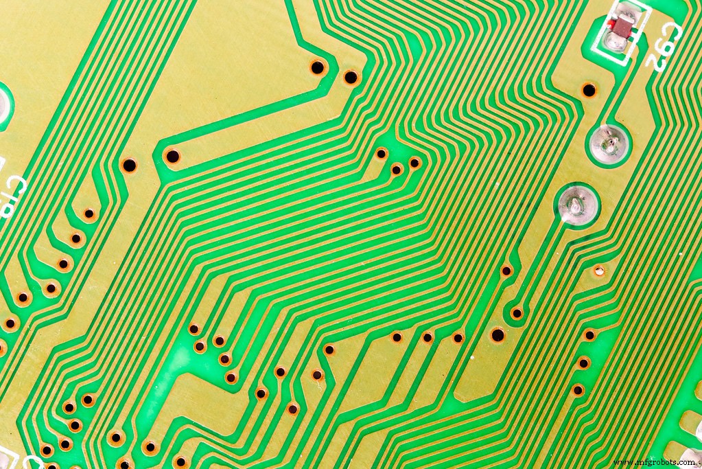
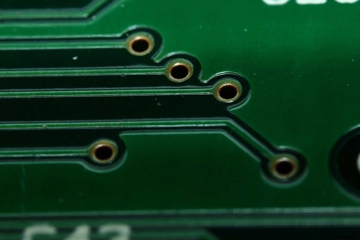
PCB Traces
Your PCBs won’t have current-carrying compatibilities without traces. But, if there are any bends or crosses on your paths, it would create an antenna. And that’s what we want to avoid.
So, here are some standard rules for trace design:
- Always put at least 3W space between your traces (W for width). Also, you must separate all signals from other paths. With this rule, you can minimize coupling and crosstalk between neighboring traces.
- Don’t use right-angle bends for your traces. You can use 45-degree angles instead. Why? Because right-angle bends can increase capacitance and change impedance value–which creates reflections.
Right-Angle Traces
- Try keeping your differential traces close when routing. It would maximize the coupling factor and control noise.
- Use vias only when necessary. You should try to avoid using vias as much as possible.
Vias can cause parasitic inductance because of the impedance difference between it and traces. But, if you can’t avoid using vias, ensure you place your ground vias close to the signal vias.
PCB Vias
- Stubs won’t work in high-frequency and sensitive traces. Stubs generate reflections and can potentially add a wavelength antenna to your circuit.
3. Use Proper Ground Planes
You must use only ground planes with low inductance values. Otherwise, it’ll cancel out your efforts to counter EMC problems.
Luckily, you get a ground plane with low inductance by increasing your PCB’s ground area. It would also help reduce crosstalk and EM generation. Let’s take a look at some of the design tips we recommend.
Note: Do not randomly connect your components to ground points. It’s not good practice.
- There’s no need to save space on your ground plane. Instead, ensure you use every inch of it to benefit from its small inductance value.
- You can’t always use ground planes for two-layered PCB. But, you can use ground grids, and the distance between them determines their inductance values.
- Indeed, long return paths are not necessary for EMC PCBs. Instead, a short return path has better EMC performance because of its lower impedance.
- Also, Isolate noisy environments with Faraday’s cage ring. You can create a faraday cage ring by including the ground on the board’s edge. Then, the cage will prevent signals from routing outside the boundary.
- In truth, split apertures can mess up your circuit, so be careful how you use them. Split apertures can create non-uniform areas that increase impedance.
- Ensure you also put low-speed circuits close to the power plane and high-speed circuits close to the ground plane.
- Don’t leave any floating copper fill areas. Always keep them grounded, or you’ll create an antenna.
4. How to Arrange your PCB Layers
Your PCB’s layer arrangements also determine its EMC performance. If you’re designing two or more layered boards, you should dedicate an entire layer to the ground plane. However, four-layer boards should have a power plane below the ground plane.
Here are some design guidelines for arranging PCB layers:
- First, use ground grids if you can’t dedicate an entire layer for the ground plane on a two-layered board.
- Next, Ensure the ground traces are parallel with your power traces, especially if using a separate plane.
- Finally, if your PCB design has more than four layers, we recommend using the following PCB arrangement: signal layer-ground layer-power layer-signal layer.
5. Make use of Shielding.
Shielding is one effective method for countering EM emissions. So, with conductive/magnetic materials, shielding covers can protect signals from external interference and prevent information loss.
We recommend using cable shielding. Why? Because cables are a significant source of EMI, especially ones that transmit analog and digital signals. Also, these cables have high parasitic capacitance and inductance.
But, you can prevent such EMI problems by using cable shielding.
5. Separate all Sensitive Components
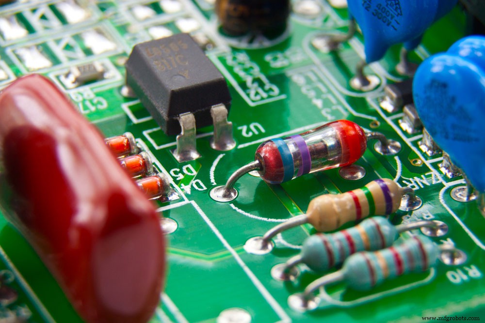
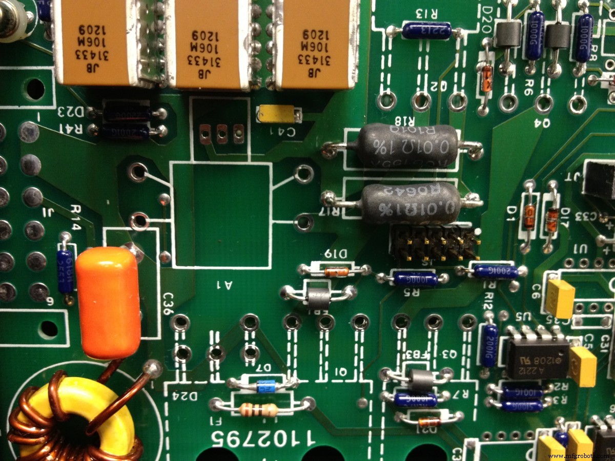
Electronic Components
You can’t achieve an EMC-friendly design by clustering all components together. Instead, separate them according to their operating signals, like digital, analog, low-speed, high-speed, and power supply signals.
Another thing to do is separate each group’s signal tracks and put them in their specific area. Plus, a filter would be great if one signal flows through different subsystems.
EMC Standards
EMC Standards
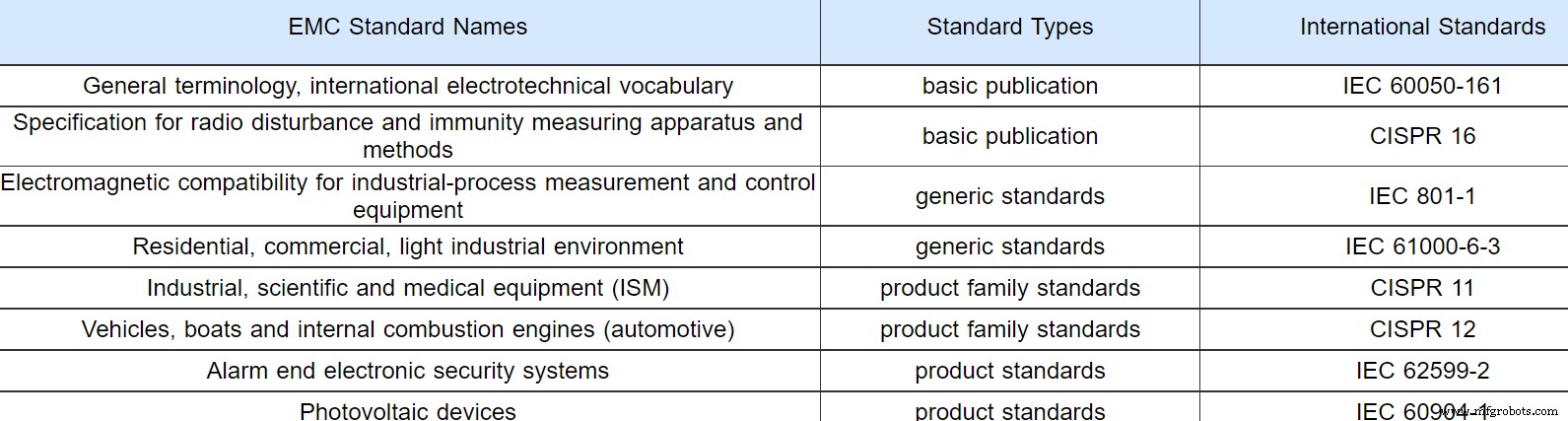
Although there are different versions of EMC standards, most get inspiration from IEC standards.
These EMC standards created two requirements that every electronic device must follow. These requirements include:
- Electronic devices must not create and transmit negative electromagnetic interference to other devices.
- Electronic devices must also resist EMI from other devices.
Click here for more information on the various EMC standards.
Other Precautions for PCB EMC Designs
Here are a few tips to help increase the performance of your EMC PCB design.
1. First, be careful when designing or locating your oscillator layouts. Hence, you must keep all oscillator tank loops far away from analog circuits, connectors, and low-speed signals. Remember that this tip applies to the board’s PCB and box space.
2. Also, you must know that not all PCBs are the same. Some designs nay may require filtered connectors to filter out noise. Plus, you must tether your connector to the chassis and PCB.
3. Next, don’t run high-speed or noisy lines near your board’s edge. Noisy traces can pick up noise easily, so you must keep them away from areas that generate noise. These areas include oscillator circuits, relay drivers, connectors, and relays.
4. Additionally, some PCBs may require filtering on some lines. An easy solution for this is ferrite beads. Ferrite beads can limit high-frequency signals and work for decoupling supply lines.
5. Remember to keep cable assemblies far away from an oscillator or a section with a microcomputer in your design. Cable assemblies can degrade your EMC’s performance because they pick and carry noise around your entire circuit.
Difference Between EMI and EMC?
As previously mentioned, EMI is any noise that corrupts other signals transmitting or receiving data or information.
Plus, there are two ways EMI can occur. One is through the air, and the other happens when a conductor transfers it to another material (conductive EMI).
In contrast, EMC is a device’s ability to withstand dangerous levels of EMI and keep operating normally. Devices with a good EMC standard won’t generate intolerable EMI and won’t have disrupted signals and operations.
Rounding Up
PCB Design
Electromagnetic interference is a powerful phenomenon that could cause loss of information and severe system disruptions. It’s similar to the fictional electromagnetic pulse that can disrupt all electronic devices within range.
However, we can counter EMI with EMC -friendly boards. These boards have a specific immunity that protects them from signal disruptions. EMC PCBs also don’t create high levels of EMI, so they don’t affect the devices around them.
Do you want to build an EMC PCB for your next project? Be sure to contact us, and we’ll be happy to help.
Industrial Technology
- Mastering PCB Electromagnetic Interference: Strategies for Reliable Design
- Castellated PCBs: The Optimal Solution for Efficient Board Assembly
- PCB Crosstalk Explained: Causes, Effects, and Effective Countermeasures
- Silkscreen on PCBs: The Essential Guide for Accurate Component Placement
- Optimizing PCB Layout for Superior EMC Performance in Electronics
- Effective EMC Strategies for PCB Design in Electronic Devices
- Optimizing High-Speed PCB Routing to Minimize EMI Impact
- Enhancing PCB Electromagnetic Compatibility: Key Strategies for Power and Ground Optimization
- Mastering PCB Interference Mitigation: A Professional Guide to Ensuring EMC Compliance
- Guarantee First‑Time Success in PCB EMC Design