


Miniaturized PCBs: Balancing Form, Function, and Reliability in Modern Electronics
Today’s electronics demand compact, low‑power packages that integrate signal processing, sensors, imaging, and power management—all within increasingly tighter dimensions and sometimes on flexible substrates. These requirements challenge traditional rigid PCBs, pushing designers toward new miniaturized formats that conform to shrinking form factors such as smartwatches, IoT devices, and wearable tech.
Designers must now navigate thinner traces, high‑speed signal paths, strict impedance control, and dense via placement—all while adapting to modified substrates and a heavier reliance on embedded components. These constraints impact reliability, functionality, power consumption, and ultimately the success of a product.
Key Design Challenges
Battery life remains paramount in compact devices. Signal loss and propagation delays can erode endurance, so designers focus on signal integrity, power management, and EMI mitigation. Flexible PCBs, in particular, suffer from impedance drift when flexed, which further stresses signal quality.
Passive components—resistors, capacitors, inductors—often must be embedded directly into the PCB due to space limits. However, embedding is still an emerging technology and can compromise reliability or performance, adding restrictions to the design flow.
Near‑field RF communication is increasingly common, demanding precision copper traces, narrow line spacing, and carefully positioned vias. Conventional RF modules, built for rigid, high‑cost substrates, no longer fit; designers must adopt thinner, more flexible materials and alternative via reinforcement to maintain signal integrity.
Innovations in Miniaturized PCB Manufacturing
Laser direct imaging (DI) has become essential for creating sub‑10‑µm traces. A top‑tier DI system balances high registration accuracy with production speed, achieving depth‑of‑focus that accommodates PCB topography changes and delivers uniform line quality. This approach offers a cost‑effective alternative to front‑end lithography and, with advances in solder mask positioning, is poised to support sub‑10‑µm features.
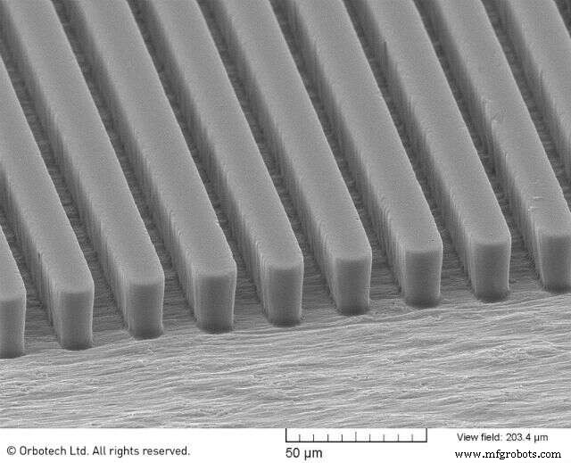
Figure. Direct Imaging now allows mSAP and advanced HDI PCB with 10 µm feature size. (Source: Orbotech)
Advanced UV laser drilling enables precise vias through a wide range of materials—including ABF, polyimide, ceramic, resin, mold compounds, metal, and solder resist—without residue or undercut. Registration accuracy of 6 µm ensures reliable interlayer connections.
These technologies streamline production for thinner, smaller, and more flexible boards, boosting precision, quality, and throughput. From a business perspective, investing in DI, UV drilling, and inspection systems improves yield, enabling suppliers to confidently produce high‑functioning miniaturized PCBs.
Gil Tidhar is the Co‑head of Orbotech’s Global Product Organization (GPO). With over 25 years of experience in electro‑optics, physics, and system engineering, he has a proven record of translating scientific advances into market‑ready systems. Gil holds multiple patents, has published several papers, and has served as a conference committee member and session chair for the SPIE DSS international annual symposium.
Embedded
- Top 13 Smart Home Devices & Systems of 2019 – Expert Picks
- The Evolution of Printed Circuit Boards: Innovations and Impact
- Metal Spinning & Hydroforming: Cost‑Effective Alternatives to Traditional Die Stamping
- Single vs. Double-Sided PCBs: Which Design Is Right for Your Project?
- Eagle vs Altium: Feature Comparison & Key Differences for PCB Designers
- In-Depth Guide to Six Key PCB Applications in Modern Electronics
- Fiducial PCB Design: Purpose, Placement, and Best Practices
- Effective EMC Strategies for PCB Design in Electronic Devices
- Why Assembling PCBs in the USA Drives Innovation and Reliability
- Why Prototyping PCBs Is Essential for Reliable Electronics