


Ceramic Substrate PCBs: Expert Insights and Design Best Practices
Generally, there’s a technological revolution resulting in discarding traditional CEM-3 and FR-4 because of poor thermal conductivity. In their stead, we have seen market demand for highly integrated circuit boards with sound dissipation systems (high heat resistance in an outdoor environment). Today’s post gives a quick overview of Ceramic Substrate PCB.
What is the Ceramic Substrate?
A ceramic substrate is a unique process PCB with thermal conductivity of 9-20W/m.k made at high temperatures under 250°C. Manufacturers prepare the substrate by directly binding copper foil to aluminum nitride (AIN) or alumina (Al2O3) surfaces.
Its electrical and thermal performance makes it better than most metal core PCBs in the PCB industry.
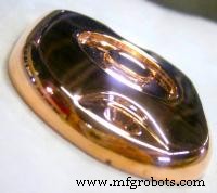
Copper plating on aluminum
Advantages of Ceramic Substrate PCB
Ceramic substrate PCB has several advantages making it ideal for multiple products like;
Material advantages
- Since the copper layer lacks an oxide layer formation, you can durably use it in a reducing atmosphere.
- Secondly, it has a tough chemical erosion resistance and versatile/hermetic packages that prevent water absorption.
- Thirdly, it has high reliability in aerospace, is resistant to cosmic rays, and does not have organic ingredients.
- Then, you can achieve high-density assembly with low thermal resistance.
- Also, it has a low high-frequency loss and good electrical insulation performance, thus able to withstand the harsh external environment.
- Besides using a high temperature during its soldering, a ceramic substrate has good solderability.
- In addition, you can safely operate it in temperatures up to 350°C.
- It is a lower and stronger electrical resistance metal film (alumina ceramic PCB).
- Further, ceramic circuit boards are cost-efficient and ideal for heavy-duty applications.
- Finally, it has a more matching thermal expansion coefficient and higher thermal conductivity.
Technical advantages
The LAM and DPC technologies are gradually replacing traditional boards like DBC and LTCC technologies for many reasons.
- For instance, laser drilling technology provides a great application value since it’s accurate, fast, and efficient.
- Then, there are good electrical properties and high bonding strength between the ceramic and metal circuit layer.
- There’s also a through-hole connection that gives customers a customized product solution.
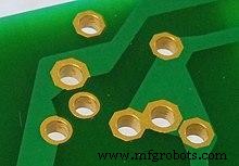
Through-hole plating on an electronic circuit board
What are the Types of Ceramic Substrates?
According to the material
Al2O3
Our first substrate is by far the most commonly utilized in the electronics industry. Reasons behind its popularity are its electrical, thermal, and mechanical properties making it chemically stable and of high strength compared to other oxide ceramics. Al2O3 is also rich in raw materials.
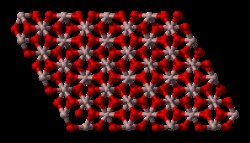
Aluminum oxide structure
Applications; The ceramic product is ideal for manufacturing several different shapes.
AlN (Aluminum Nitride ceramic board)
AlN ceramic-based printed circuit board has two significant features worth knowing;
- Expansion coefficient matching Si.
- High thermal conductivity.
However, it has disadvantages like being pricier than Al2O3 and even a thin oxide surface layer affecting its thermal conductivity. Fortunately, you can control the process and materials while manufacturing AlN substrate to get a product with good consistency. Also, technological advancements might soon consider the pricing of Aluminum nitride boards.
Applications; Substrates for electronic materials (packages) and heat sinks to transfer heat from hot spots.
BeO
Compared to metal aluminum, BeO has higher thermal conductivity and is suitable for applications needing high thermal conductivity.
Also, remember that it is sometimes toxic and, therefore, not commonly developed.
Conclusion; Alumina ceramics, as we have seen, have properties and superior comprehensive performance that still make them dominant in various fields. For example, you will find them in power modules, hybrid microelectronics, and power electronics.
They provide high mechanical strength, chemical stability, good dielectric properties, and thermal properties.
According to the manufacturing process
Co-fired ceramic microelectronic
High-Temperature Ceramic PCB/High-Temperature Co-Fired Multilayer Ceramic (HTCC) circuit
This PCB type can withstand high temperatures (above 1300 Degrees Celsius). The unique manufacturing process involves creating new ceramics by combining lubricant, aluminum oxide, adhesive, plasticizer, and solvent.
Afterward, manufacturers coat the new ceramic and apply a circuit pattern tracing on tungsten, manganese, or molybdenum precious metals. They bake the circuit boards for about 48 hours at temperatures ranging from 1300 to 1700°C after lamination in a gaseous environment with hydrogen gas.
However, because of high co-firing temperatures, it lacks many metal conductor materials.
Low-Temperature Ceramic PCB/Low-Temperature Co-Fired Ceramic (LTCC) circuit
Manufacturers use crystal glass materials and adhesive substances (organic binder) to create low-temperature ceramic PCBs. They apply both materials to a metal sheet that has gold paste. Then, they cut and laminate the board before placing the PCB in a gaseous oven at 900°C.
Advantages
- It has less warpage and better shrink than HTCC.
- Additionally, it has higher mechanical intensity and thermal conductivity than other substrate types.
Applications; Heat-free products like LED lights.
Thick Film Ceramic PCB
In a thick film process, manufacturers coat gold and dielectric pastes on a ceramic base material. Then, they bake the material at 1000°C or lower operating temperature. They prefer a thick film ceramic due to its ability to prevent copper oxidation.
Thus, the manufacturers can use electronic components like resistors, electric capacitors, conductors, semiconductors, and interchangeable conductors on the ceramic board.
Thick film technology
Often, it is a preferred choice when worried about oxidation. Also, the conductive layer of thick film ceramic PCB board shouldn’t be thicker than 13 microns.
- DBC (Direct Bonded Copper)
The technology utilizes an oxygen-containing eutectic solution of copper to place metal copper on the ceramic circuit board directly. Often, its basic principle involves introducing a required amount of O2 between ceramic and copper during or after a deposition process. The two materials form a Cu-O eutectic liquid in thermal ranges between 1065 to 1083°C.
- DPC (Direct Plate Copper)/ Copper-plated substrate
The ceramic material option often undergoes the process below;
Manufacturers begin by pre-processing and cleaning the ceramic substrate. Then, they use a professional film manufacturing technology-vacuum coating method to sputter and bond a copper metal composite layer onto the substrate.
Next, the photoresistor with yellow light lithography undergoes re-exposure, development, and etching. Finally, the film removal process becomes complete, and now the manufacturers increase the circuit thickness by electroless/electroplating plating deposition.
Removing the photoresist completes the metallization circuit.
- LAM (Laser Activation Metallization)
The rapid laser technology ionizes meta and ceramic using a high-energy laser beam. Afterward, it lets the two components grow together, enhancing their firmness during the metallization process.
Application of Ceramic PCB
Due to its features like high thermal conductivity, low dielectric constant, etc., ceramic PCBs are in the applications listed below;
- Street, high bright light,
- Semiconductor process equipment,
- Telecom devise,
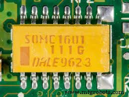
- Sensor,
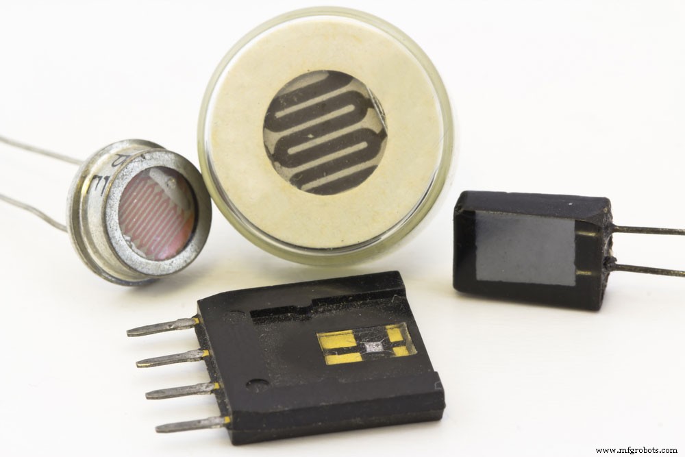
(different types of sensors)
- Solar cell,
- Automotive light system,
- LEDs,
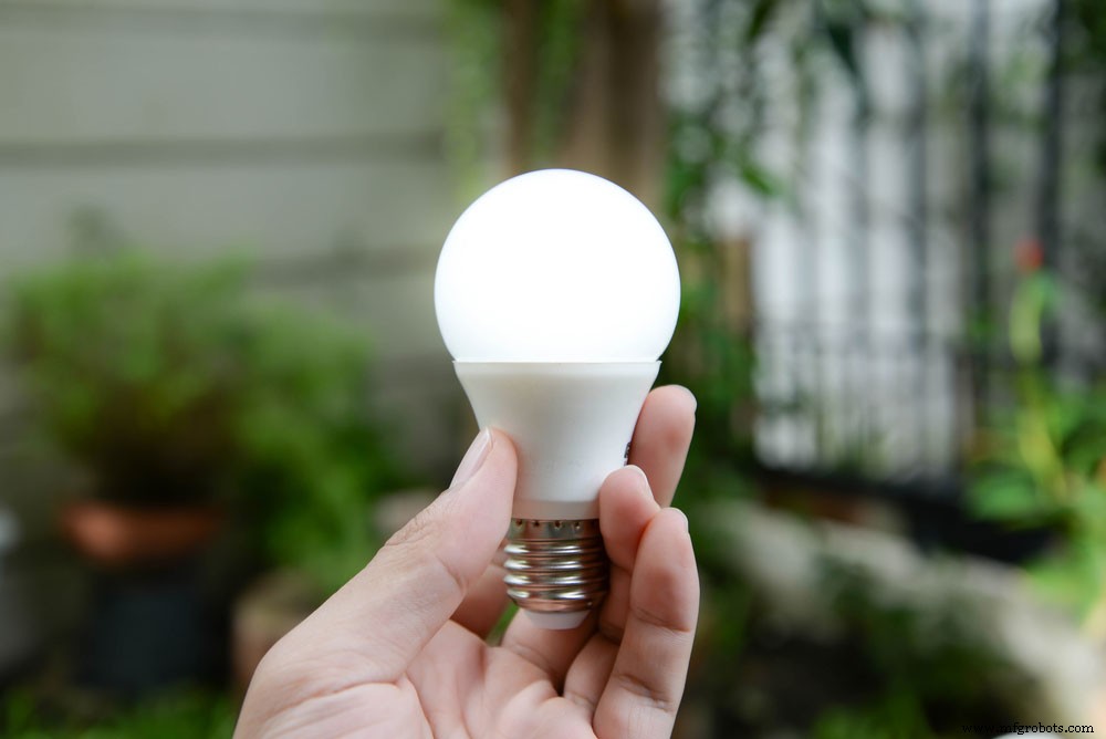
(LED bulb)
- Digital and Analog PCB,
- Transmission/Receiving module,
- Solar panel arrays,
- Solid-state relay (SSR),
- High-accuracy clock oscillator, OCXOs, TCXOs, VCXOs,
- High-power circuits,
- Chip-on-board module, and
- Memory module.
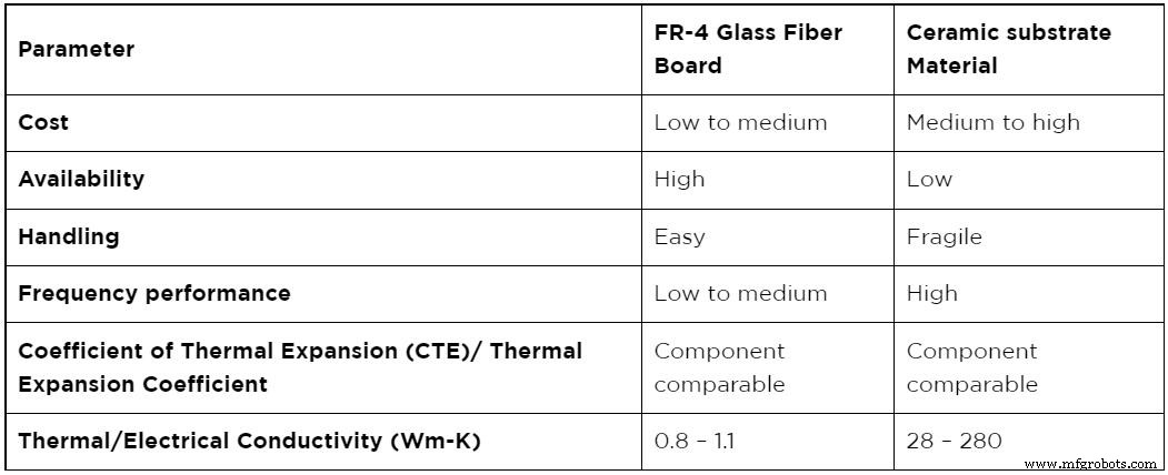
Ceramic PCB VS FR4
We’ll now compare the ceramic multilayer and FR4 board materials based on several criteria below.
Conclusion
In conclusion, ceramic circuit boards are efficient in several industries, like the electronic industry depending on your manufacturing needs and designs. They also provide quality features like thermal efficiency, good electrical conductivity, and mechanical strength.
Kindly contact us if you wish to know more about ceramic substrate materials.
Industrial Technology
- Choosing the Right PCB Material: A Comprehensive Guide
- Mastering PCB Stiffeners: A Complete Guide for Flex PCBs
- Comprehensive Guide to PCB Testing Methods: Ensuring Quality & Reliability
- PCB Gold Fingers: Comprehensive Guide & Specifications
- Understanding Moisture Sensitivity in PCBs: Prevention, Detection, and Removal
- Comprehensive Guide to PCB Temperature Management
- Complete Guide to Printed Circuit Board Assembly (PCBA)
- Master PCB Laminates: The Definitive Guide for Engineers
- Sark 110 Antenna Analyzer: Full Feature Guide
- Mastering High-Speed PCBs: A Complete Design Guide