


Presensitized PCBs: A Comprehensive Manufacturing Guide
Printed circuit boards (PCBs) are the foundation of every modern electronic device. Whether you’re new to PCB design or a seasoned repair technician, understanding how presensitized PCBs are made and why they’re preferred in high‑volume production is essential.
What Is a Presensitized PCB?
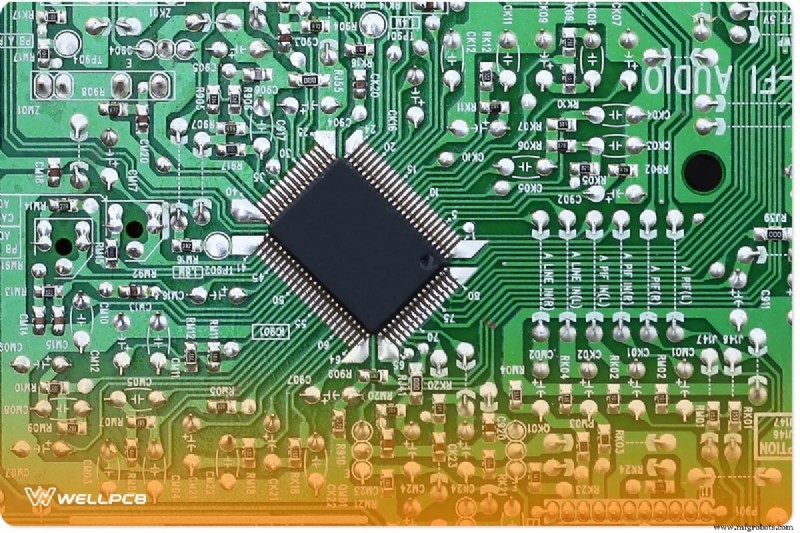
A presensitized PCB is a factory‑made board whose copper surface is coated with a photosensitive emulsion. This coating allows the board to be exposed to ultraviolet (UV) light, enabling the creation of precise copper traces in a single step. Today, the vast majority of commercial electronics—from smartphones to industrial controls—use presensitized PCBs because of their speed, consistency, and cost‑effectiveness.
Design and Manufacturing Process of Presensitized PCBs
Ready to replicate the quality of a professional PCB in your workshop? Follow this step‑by‑step workflow that mirrors industry best practices.
Materials You’ll Need
- Exposure box with UV LEDs
- Precision drill bits (0.8 mm & 1.2 mm)
- Ferric chloride (FeCl₃) solution
- Sodium hydroxide (NaOH) bath
- Protective eyewear, gloves, lab coat
- Tin solution for tinning
- Acetone for resin removal
- Water bath (distilled water)
- Timer, buckets, power supply, dust coat, solder
Design Your PCB
Use professional CAD tools such as Proteus or the open‑source Fritzing to layout your board. Export the final design as a 1:1 PDF—this preserves scale and ensures the printed mask matches the board dimensions.
Print the Mask
Print three copies of the design onto clear acetate using a laser printer. Mirror the top layer, dimensions, vias, and pads so the pattern aligns correctly on the copper surface. Multiple copies provide redundancy and improve opacity during exposure.
Prepare the Chemical Bath
Safety first: wear gloves, goggles, and a lab coat in a well‑ventilated area. Prepare a 30 % ferric chloride solution to dissolve copper and a 10 % NaOH bath for development. Keep a distilled water bath ready for rinsing between steps.
Exposure
Place the copper board face‑down on the masked acetate. Secure with tape and slide the assembly into the UV exposure box. Expose for 2 to 2½ minutes—adjust based on lamp intensity. After exposure, remove the board carefully, peel off the protective film, and rinse in distilled water.
Development
Immerse the board in the NaOH bath for 30–60 seconds. The unexposed emulsion turns blue‑purple (or grey), revealing the copper pattern. Rinse thoroughly with water and dry.
Etching
Submerge the developed board in the ferric chloride bath. Stir gently; copper will dissolve in 20–40 minutes, depending on temperature and surface area. Once the desired traces appear, remove the board, rinse in water, and dry.
Resin Removal
Soak the board in acetone for 10–20 seconds to dissolve residual photoresist. After the acetone turns yellow, rinse with water and scrub lightly to ensure all organic material is gone.
Tinning (Optional but Recommended)
Dip the board in a tin‑II chloride solution to deposit a thin tin layer. This protects the copper, prevents corrosion, and improves solderability.
Drilling
Use a vertical drill press with 0.8 mm bits for standard holes. If components require larger vias, switch to a 1.2 mm bit. Take care to keep the drill perpendicular to avoid misalignment.
Etching Presensitized PCBs: Tips and Best Practices
Etching is the critical step that defines the final trace geometry. Follow these guidelines for clean, precise results:
- Maintain a clean workbench—dust and debris can cause irregular copper removal.
- Use freshly prepared ferric chloride; its potency drops over time.
- Stir the bath continuously to keep copper ions in solution.
- After etching, immediately rinse the board in water to stop the reaction.
UV Photoresist Chemistry in Presensitized PCBs
The photosensitive layer reacts to UV light: in a positive photoresist, exposed areas dissolve; in a negative resist, exposed areas harden. Most presensitized PCBs use a negative resist, where the mask blocks UV, leaving copper exposed only in the unmasked areas. This process yields high‑resolution, defect‑free traces suitable for complex circuits.
Advantages of Presensitized PCBs
- Compact Design – Copper traces replace bulky wiring, saving space and weight.
- Rapid Prototyping – One‑step exposure and etching drastically cut manufacturing time.
- High Reliability – Consistent copper thickness and precise trace geometry improve performance.
- Easy Repair – Faulty components can be replaced without rewiring the entire board.
- Strong Component Mounting – Tin plating and solder joints secure components against vibration and movement.
Conclusion
Presensitized PCBs combine speed, precision, and cost savings, making them the industry standard for everything from consumer gadgets to mission‑critical systems. By following the steps outlined above, you can produce high‑quality boards in your own workshop or order ready‑to‑use boards from a trusted supplier like WellPCB.
Industrial Technology
- Precision Metal Fabrication – Small to Large Projects
- EPA Method 21: Comprehensive Leak Detection & Repair Protocol
- Top 12 Starlink Alternatives in 2026: Leading Satellite Internet Competitors
- Comprehensive PCB Testing: In‑Circuit & Functional Reliability Assurance
- Maximize Efficiency: How Asset Tracking Saves Time and Money
- Mastering Dovetail Joints: Techniques, Tools & Tips for Strong Woodworking Connections
- LED Fader Circuit Explained: How It Works & Why It Matters
- 3 Key Benefits of Mobile Building Maintenance Management
- Mastering HR Challenges in Manufacturing: Proven Strategies for Success
- Top 6 Benefits of Ball Grid Array (BGA) Packaging for PCBs