


Modeling Data Converters for Accurate System Simulations
Modeling Data Converters for Accurate System Simulations
Engineers routinely face tight design schedules that leave little time to answer key questions about data‑converter performance. This series addresses those questions, beginning with a foundational exploration of how to model analog‑to‑digital (ADC) and digital‑to‑analog (DAC) converters for system‑level simulations.
In prior work, the author examined whether I/Q combining should be performed digitally or analogly, and outlined requirements for robust communications‑link performance. The current article builds on that foundation by exploring how to quantify and model the critical parameters of DACs and ADCs in direct‑RF sampling architectures.
Direct‑RF Modulation and Demodulation
Figure 1 demonstrates two common topologies: direct RF DAC conversion for modulation and direct RF ADC conversion for demodulation. The DAC and ADC together are referred to as data converters.
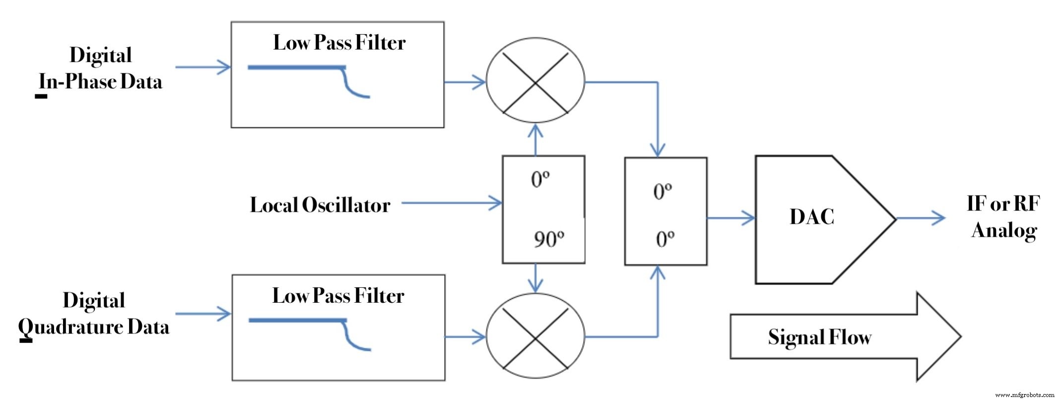
Figure 1(a). Modulator
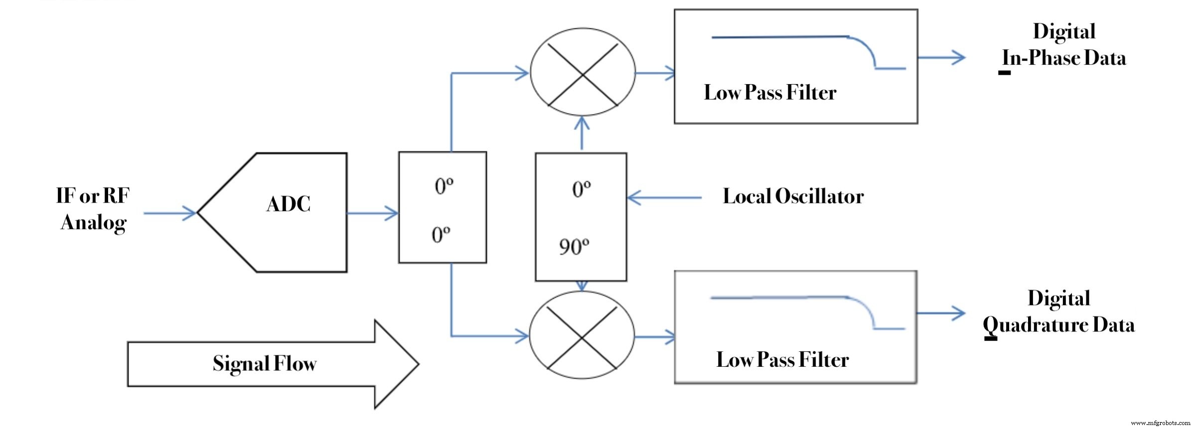
Figure 1(b). Demodulator
Although the link‑level impact of data‑converter non‑idealities is well documented, the specific quality requirements for DACs and ADCs in this configuration remain under‑explored in the literature.
Why Simulate Data Converters?
Bit‑error‑rate (BER) studies demand statistically meaningful results, typically requiring several hundred to a thousand error events. For a target BER of 10-4, this translates to 5 million bits of simulated data. Achieving such throughput necessitates a concise, yet comprehensive, converter model that captures the most influential characteristics without excessive computational overhead.
This article presents a systematic approach to modeling, split into ADC‑centric and DAC‑centric sections. Note that sigma‑delta converters are excluded in this discussion.
Models for Analog‑to‑Digital Converters (ADCs)
Key references ([4]–[18]) cover analysis, modeling, and testing of high‑speed ADCs. In particular, studies such as [13], [14], [16], and [17] introduce advanced models that capture nonlinear behavior. However, many engineers still seek a simpler, more intuitive representation that remains faithful to real‑world performance.
Figure 2 illustrates the quantization process of a 5‑bit bi‑polar ADC, which has 32 discrete output levels. The peak voltage spans +0.9375 V to –1.0 V, approximately ±1 V. RF engineers typically work with RMS values; a sine wave of 1 V peak has an RMS of 0.707 V, which is –3 dB relative to full scale. To avoid confusion, we introduce two units: dBpeakFS for peak‑to‑full‑scale ratios, and dBrmsFS for RMS‑to‑full‑scale ratios.
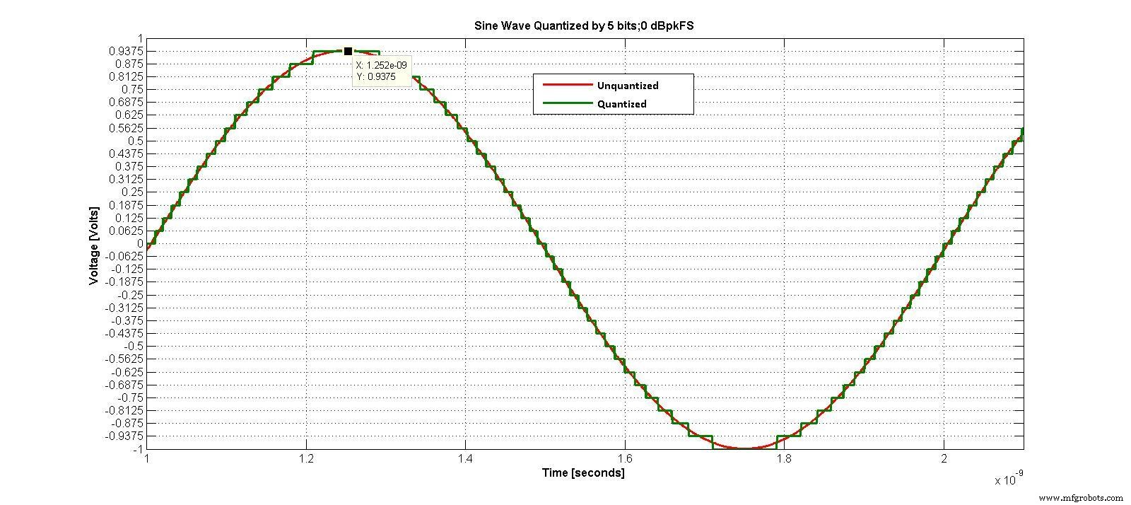
Figure 2.
Bandwidth selection is another critical consideration. Traditional audio ADCs focus on the full Nyquist bandwidth, but direct‑RF sampling requires only the portion occupied by the signal plus guard bands. We define the "interesting bandwidth" as the region that will be processed by the digital signal processor (DSP). Figure 3 visualizes this concept.
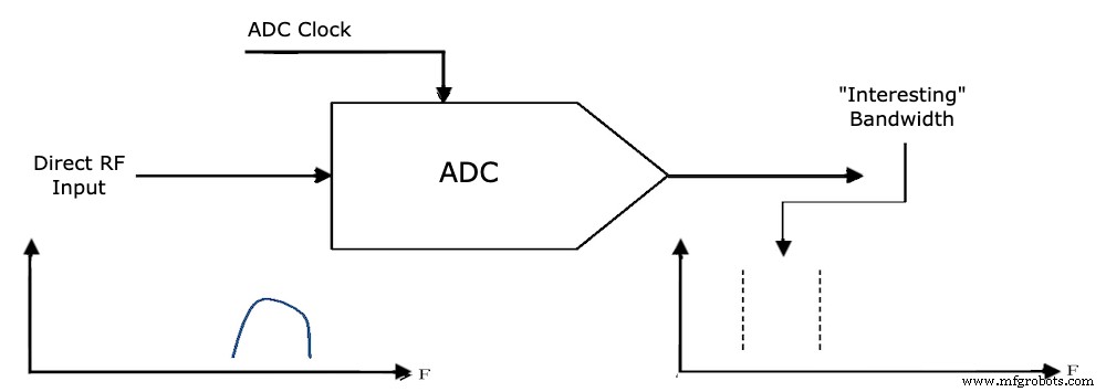
Figure 3.
In this figure, the signal bandwidth and the interesting bandwidth may coincide in width but differ in center frequency due to band‑pass sampling, where the ADC clock (fS) serves as a mixer’s local oscillator. The Nyquist frequency is fNyquist = fS/2.
Choosing an Input Signal for Model Development
Characterizing an ADC requires a test signal that exposes its dynamic behavior. While a single‑tone sine wave is common in datasheets, it offers zero bandwidth and no amplitude variation. A two‑tone input, shown in Figure 4, provides both bandwidth and amplitude modulation, making it a practical choice for both hardware testing and simulation. Many manufacturers also provide performance data for two‑tone stimuli.
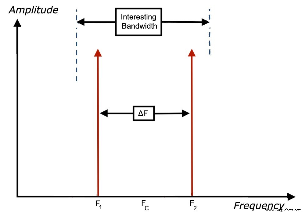
Figure 4.
Other signal shapes—Gaussian spectra, AM, FM—have been proposed in the literature ([4], [12]). These are less common in commercial test suites but can be valuable for specialized applications.
In the next article of this series, we will introduce an ADC model based on the Effective Number of Bits (ENOB). Until then, readers may consult the abbreviations, glossaries, and references provided below.
Abbreviations Used
Glossaries
- Munson, Justin; "Understanding High Speed DAC Testing and Evaluation"; Analog Devices Application Note AN-928; 2013
- Arrants, Alex; Brannon, Brad; & Reeder, Rob; "Understanding High Speed ADC Testing and Evaluation"; Analog Devices Application Note AN-835; 2010
- Baker, Bonnie; "A Glossary of Analog‑to‑Digital Specifications and Performance Characteristics"; Texas Instruments Application Report SBAA147B; 2011
- Malobert, Franco; Data Converters; Springer Publishing; Chapters 2 and 9
- Myderrizi, I; Zeki, A; "Current‑Steering Digital‑to‑Analog Converters: Functional Specifications, Design Basics, and Behavioral Modeling"; IEEE Antennas and Propagation Magazine, vol.52, no.4, 2010
References
- [1] Brodsky, Wesley; "Should I and Q Combining and Separation be done Digitally or Analogly?"; WBWC.01; 2014
- [2] Maloberti, Franco; Data Converters; Springer Publishing; 2007
- [3] VanTrees, Harry L; Detection, Estimation, and Modulation Theory, Part III; 1971
- [4] Seokjin Kim; Elkis, R.; Peckerar, M.; "Device Verification Testing of High‑Speed ADCs in Satellite Communication Systems"; IEEE Trans. Instrum. Meas.; 2009
- [5] Vedral, J.; Fexa, P.; Svatos, J.; "Using AM and FM signals for ADC testing"; I2MTC 2010
- [6] Kester, Walt; "The Good, the Bad, and the Ugly Aspects of ADC Input Noise—Is No Noise Good Noise?"; Analog Devices Tutorial MT‑004; 2008
- [7] Arrants, A.; Brannon, B.; Reeder, R.; "Understanding High Speed ADC Testing and Evaluation"; Analog Devices AN‑835; 2010
- [8] Kester, Walt; "Understand SINAD, ENOB, SNR, THD, THD+N, and SFDR"; Analog Devices MT‑003; 2008
- [9] Shinagawa, M.; Akazawa, Y.; Wakimoto, S.; "Jitter analysis of high‑speed sampling systems"; IEEE J. Solid‑State Circuits; 1990
- [10] Hummels, D.M.; Irons, F.H.; Cook, R.; Papantonopoulos, I.; "Characterization of ADCs using a non‑iterative procedure"; IEEE Trans. Circuits and Systems; 1994
- [11] de Mateo Garcia, J.C.; Armada, A.G.; "Effects of bandpass sigma‑delta modulation on OFDM signals"; IEEE Trans. Consumer Electronics; 1999
- [12] Abuelma'atti, M. T.; "Effect of Nonmonotonicity on the Intermodulation Performance of A/D Converters"; IEEE Trans. Commun.; 1985
- [13] Traverso, P.A.; Mirri, D.; Pasini, G.; Filicori, F.; "A nonlinear dynamic S/H‑ADC device model based on a modified Volterra series"; IEEE Trans. Instrum. Meas.; 2003
- [14] Fraz, H.; Bjorsell, N.; Kenney, J.S.; Sperlich, R.; "Prediction of Harmonic Distortion in ADCs using dynamic Integral Non‑Linearity model"; BMAS 2009
- [15] Kester, Walt; "ADC Noise Figure—An Often Misunderstood and Misinterpreted Specification"; Analog Devices MT‑006; 2014
- [16] Brannon, B.; MacLeod, T.; "How ADIsimADC Models an ADC"; Analog Devices AN‑737; 2009
- [17] Dardari, D.; "Joint clip and quantization effects characterization in OFDM receivers"; IEEE Trans. Circuits and Systems I; 2006
- [18] Lavrador, P.M.; de Carvalho, N.B.; Pedro, J.C.; "Evaluation of signal‑to‑noise and distortion ratio degradation in nonlinear systems"; IEEE Trans. Microwave Theory and Techniques; 2004
- [18A] Gray, R.M.; "Quantization Noise Spectra"; IEEE Trans. Information Theory; 1990
- [19] Wikner, J.J.; Tan, N.; "Modeling of CMOS digital‑to‑analog converters for telecommunication"; IEEE Trans. Circuits and Systems II; 1999
- [20] Angrisani, L.; D'Arcò, M.; "Modeling Timing Jitter Effects in DACs"; IEEE Trans. Instrum. Meas.; 2009
- [21] D'Apuzzo, M.; D'Arcò, M.; Liccardo, A.; Vadursi, M.; "Modeling DAC Output Waveforms"; IEEE Trans. Instrum. Meas.; 2010
- [22] Myderrizi, I.; Zeki, A.; "Current‑Steering DACs: Functional Specifications, Design Basics, and Behavioral Modeling"; IEEE Antennas and Propagation Magazine; 2010
- [23] Lee, S.M.; Taleie, S.M.; Saripalli, G.R.; Seo, D.; "Clock‑Phase‑Noise‑Induced TX Leakage Estimation of a Baseband Wireless Transmitter DAC"; IEEE Trans. Circuits and Systems II; 2012
- [24] Naoues, M.; Morche, D.; Dehos, C.; Barrak, R.; Ghazel, A.; "Novel behavioral DAC modeling technique for WirelessHD system specification"; ICECS 2009
- [25] Bae, K.; Shin, C.; Powers, E.J.; "Performance Analysis of OFDM Systems with Selected Mapping in the Presence of Nonlinearity"; IEEE Trans. Wireless Communications; 2013
- [26] Ling, W.A.; "Shaping Quantization Noise and Clipping Distortion in Direct‑Detection Discrete Multitone"; Lightwave Technology; 2014
- [27] Engel, G.; Fague, D.E.; Toledano, A.; "RF digital‑to‑analog converters enable direct synthesis of communications signals"; IEEE Commun. Mag.; 2012
- [28] Pearson, C.; "High Speed, Digital to Analog Converters Basics"; Texas Instruments SLAA523A; 2012
- [29] Munson, J.; "Understanding High Speed DAC Testing and Evaluation"; Analog Devices AN‑928; 2013
Internet of Things Technology
- Symphony Link: Reliable Water Leak Detection for Data Centers
- Preparing Your Manufacturing Operations for AI with IoT
- Selecting Microcontroller Peripherals for High‑Performance DSP Projects
- Mastering Data Acquisition for IoT Product Managers
- Is Your Manufacturing Facility Ready for IoT? A Practical Guide
- Cut IT Support Costs in Multi‑User Computing Environments with Reboot‑to‑Restore Solutions
- How IoT Drives Smart Infrastructure to Transform Cities
- IoT-Driven Ambient Monitoring: Transforming Patient Care
- How IoT Revolutionizes Vehicle Tracking Systems
- Enhancing CNC Program Precision with External Input Integration