


Rectification and Photodetection in Si Nanowire Devices Aligned by DC Dielectrophoresis Across Platinum Electrodes
Abstract
We present a simple, scalable fabrication route for silicon nanowire (Si NW) devices in a metal‑nanowire‑metal architecture using direct‑current dielectrophoresis (DC‑DEP). The resulting devices exhibit clear rectifying I‑V characteristics, whose polarity depends on the voltage‑sweep direction. This behavior originates from asymmetric Joule heating during electrical measurements. When operated in reverse bias, the devices show pronounced photoresponse due to a strong built‑in field at the Si NW/Pt interface, suggesting potential use in photodetectors, logic elements, and sensors.
Background
One‑dimensional semiconductor nanowires possess high surface‑to‑volume ratios, quantum confinement, and exceptional crystal quality, enabling applications in photovoltaics, LEDs, and photodetectors. Silicon nanowires (Si NWs) have been integrated into devices such as solar cells, LEDs, and photodetectors, leveraging their tunable electrical and optical properties.
Si NWs can be synthesized via bottom‑up methods (VLS, MBE, laser ablation) or top‑down approaches (DRIE, MACE). A recent high‑throughput method combines metal‑assisted chemical etching (MACE) with nanosphere lithography (NSL) to produce uniform Si NW arrays.
Dielectrophoresis (DEP) is widely employed to align nanowires across electrodes, enabling the fabrication of metal‑semiconductor‑metal devices. DEP aligns dielectric nanostructures by inducing dipoles in a non‑uniform AC electric field, providing precise control over orientation and placement. Prior studies on ZnO, Si, and III–V nanowires have reported rectifying I‑V behavior, often attributed to asymmetrical Schottky barriers or contact differences.
Understanding the role of Si NW/metal contacts is essential for device integration. Here, we fabricate Si NW devices using DC‑DEP and systematically investigate their electrical and photosensing properties, revealing rectifying behavior and asymmetric Joule‑heating‑induced effects.
Experimental
Si NWs were fabricated by MACE combined with NSL on n‑type Si(100) wafers (1–10 Ω cm). After standard RCA cleaning and Piranha treatment, a monolayer of 220 nm polystyrene spheres was assembled and reduced in size by O₂ plasma. A 20 nm Ag film was sputtered and etched in HF/H₂O₂ (5 M/0.176 M) at 25 °C for 15 min. Residual spheres and Ag were removed in THF and HNO₃, yielding large‑area ordered Si NW arrays. FESEM and HRTEM confirmed single‑crystalline [100] orientation and uniform diameters (150–200 nm) and lengths (5–6 µm).
For device fabrication, Pt (40 nm)/Ti (15 nm) electrodes were patterned on a heavily doped n‑type Si(100) substrate (0.001–0.006 Ω cm) via lithography, with a 2 µm gap. Si NWs were sonicated from the etch mask into isopropyl alcohol and dispersed. A droplet of this suspension was applied to the electrodes; a +0.5 V DC bias was applied to the drain during DC‑DEP alignment, with the source grounded. Electrical transport was measured using a Keithley 2612A source meter. Photoresponse was recorded under 825 mW cm⁻² broadband white light from an Hg–Xe lamp.
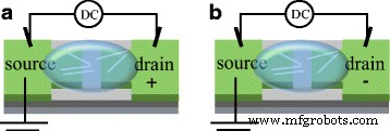
Schematics of Si NW alignment by DC‑DEP across Pt electrodes. The drain electrode is biased positively (a) or negatively (b). The source is grounded.
Results and Discussion
SEM images (Fig. 2a,b) confirm uniform Si NW arrays. TEM (Fig. 2c,d) shows single‑crystalline structure with lattice spacing consistent with Si[100].
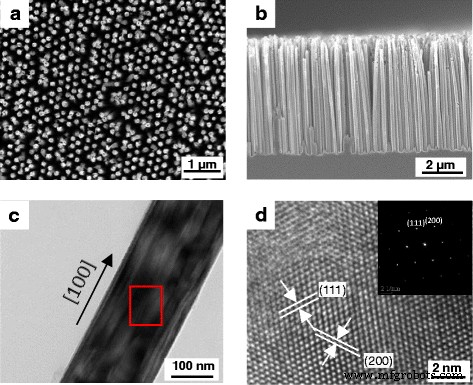
a) Top‑view SEM; b) Cross‑sectional SEM; c) TEM; d) High‑resolution TEM with SAD pattern.
Devices were aligned under a +0.5 V DC bias. SEM (Fig. 3) reveals parallel NWs bridging the Pt electrodes. By varying the IPA concentration, NW density was controlled. I‑V measurements were performed with two sweep protocols: (i) positive→negative and (ii) negative→positive. Remarkably, the rectification polarity depended on the sweep direction (Fig. 5). Wider voltage ranges enhanced rectification (on/off ratios up to 200). Repeated sweeps reinforced the rectifying behavior, indicating that the effect arises during electrical measurement rather than DEP alignment.
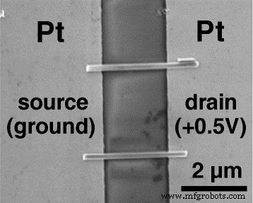
Aligned Si NWs across Pt electrodes under +0.5 V DC during DC‑DEP.
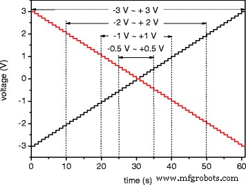
Voltage sweep rates for negative→positive (black) and positive→negative (red) bias.
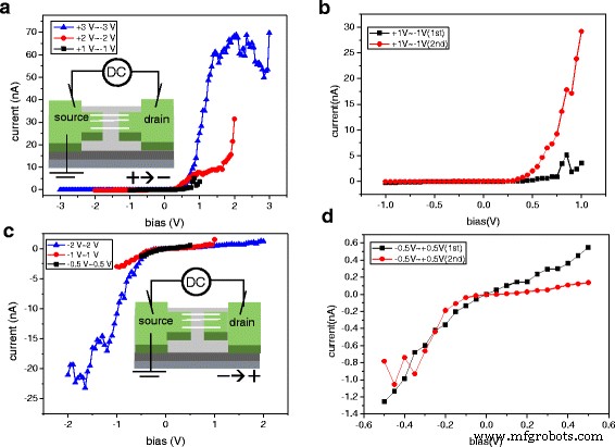
a) I‑V curves for 24 NWs (positive→negative sweep). b) First and second sweeps (+1→–1 V). c) I‑V curves for 18 NWs (negative→positive sweep). d) First and second sweeps (–0.5→+0.5 V).
The zigzag‑shaped I‑V curves observed under large‑voltage sweeps are attributed to asymmetric Joule heating. As current flows, the anode side reaches a higher temperature than the cathode, leading to local oxidation of Si and increased barrier height at the anode contact. SEM after +3 V and –3 V DEP alignment (Fig. 6) shows pronounced damage on the anode side, confirming this asymmetry.
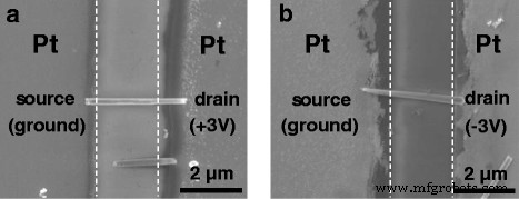
a) After +3 V alignment; b) After –3 V alignment. Dashed lines mark electrode edges.
Measurements in a reducing atmosphere (H₂/Ar) suppressed rectification over ±3 V sweeps, yielding nearly linear I‑V curves. This suggests that gas adsorption modifies the interfacial barrier. In air, oxidation at the anode during high‑temperature sweeps increases the barrier, reinforcing rectification.
Energy band diagrams (Fig. 7) illustrate the evolution: initially, symmetric, low Schottky barriers at both contacts. After asymmetric Joule heating, the anode barrier rises, causing rectification aligned with the sweep direction.
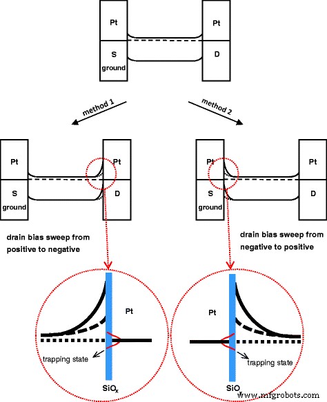
Schematic band diagrams for n‑Si/Pt contacts before (top) and after (left/right) asymmetric Joule heating in sweep protocols 1 and 2.
Photoresponse tests (Fig. 8) show that reverse bias yields a substantial photocurrent increase (≈13×) compared to forward bias. The reverse‑biased device achieves rapid rise (64 ms) and recovery (48 ms) times, thanks to the enlarged depletion region and strong built‑in field, which efficiently separates photogenerated carriers.
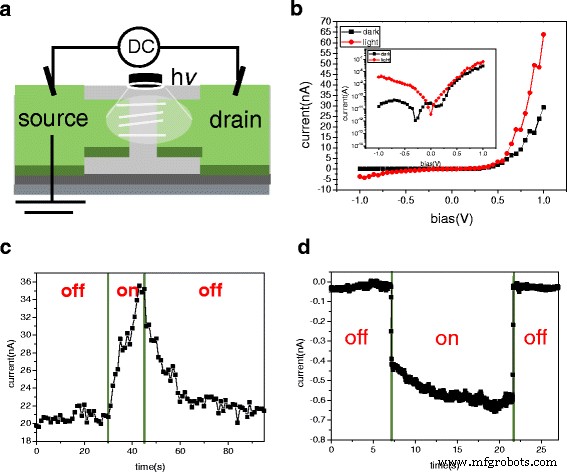
a) Device schematic under 825 mW cm⁻² illumination; b) I‑V curves in dark and illuminated conditions (semi‑log inset). c) Time‑resolved response at +0.75 V (forward bias). d) Time‑resolved response at –0.75 V (reverse bias).
Conclusions
We have demonstrated that Si NW devices fabricated via DC‑DEP across Pt electrodes exhibit voltage‑sweep‑dependent rectification due to asymmetric Joule heating during electrical measurements. In reverse bias, these rectifying devices display fast, high‑sensitivity photodetection, making them attractive for photodetectors, logic circuits, and sensor applications.
Nanomaterials
- Overcoming 4 Key IoT Challenges: Power, Connectivity, Hardware, and Integration
- Low‑Power Silicon Cochlea Enables Ultra‑Efficient Voice‑Activated Sensing
- Heating‑Enhanced Dielectrophoresis Yields Ultrahigh‑Density, Aligned Single‑Walled Carbon Nanotube Films
- High‑Performance Flexible Transparent Electrodes from Silver Nanowires with Tailored Aspect Ratios
- Optimizing Photovoltage in Metamorphic InAs/InGaAs/GaAs Quantum Dot Heterostructures: Design Insights for Light‑Sensitive Devices
- High‑Performance Quasi‑Solid‑State Asymmetric Supercapacitors Based on MoS₂/MWCNT and PANI/MWCNT Composite Electrodes
- Joule Heating Impact on Resistive Switching in Thermally Oxidized AlOx Memory Cells
- Enhancing Thermoelectric Performance: Silicon Substrates with Highly Doped Porous Si via Metal-Assisted Chemical Etching
- Efficient Fabrication of ZnO Nanowire Rectifiers via DC Dielectrophoresis Alignment Across Au Electrodes
- Harnessing Indoor Solar Power for Smart Devices