


Thermal Annealing Enhances Emission in InP/ZnS Quantum Dot Films: Photoluminescence Insights
Abstract
We investigated how post‑thermal annealing improves the optical performance of InP/ZnS core/shell quantum dot (QD) films. Emission intensity increased after annealing at 180 °C for 5 min. Temperature‑dependent photoluminescence (TDPL) and power‑dependent PL measurements revealed that the low‑energy shoulder corresponds to localized‑state emission, while the high‑energy peak arises from free‑carrier recombination. For the 180 °C‑annealed sample, the full width at half maximum (FWHM) of the localized‑state emission remained nearly constant up to 250 K before narrowing with further temperature rise, whereas the untreated film showed a pronounced FWHM reduction with temperature. These observations suggest that thermal annealing modifies the distribution of localized states, enhancing free‑carrier emission and improving device‑relevant optical properties. The findings are pertinent to the development of quantum‑dot electroluminescence and down‑conversion light‑emitting devices.
Introduction
Colloidal quantum dots (QDs) are pivotal in displays, spectroscopy, sensing, LEDs, lasers, photo‑electrochemistry, and biolabeling. InP‑based QDs offer a Cd‑free alternative with a band‑gap comparable to CdSe and full visibility across the visible spectrum, while mitigating toxicity concerns. However, InP QDs typically exhibit broader size distributions, with PL FWHM values of 50–100 nm versus 20–30 nm for Cd‑based QDs, limiting spectral purity.
Low photoluminescence quantum yields (< 1 %) stem from surface traps, dangling bonds, crystal stacking faults, and high activation barriers for trapping centers. Strategies to boost emission include surface ligand modification, epitaxial shell growth, and thermal annealing. Annealing can remove organic ligands, reduce inter‑dot spacing, and improve electronic coupling, thereby altering recombination dynamics and enhancing device performance. A systematic understanding of how annealing affects carrier recombination in core/shell QDs is essential.
In this study, we fabricated InP/ZnS core/shell QD films by spin‑coating and subjected them to post‑annealing at various temperatures. PL spectra at 300 K revealed that only the sample annealed at 180 °C displayed enhanced emission. Subsequent temperature‑ and power‑dependent PL analyses compared untreated and 180 °C‑annealed films, elucidating the origins of the spectral features and the impact of annealing.
Methods
InP/ZnS nanocrystals were synthesized following established protocols. A 0.45 mmol solution of indium(III) chloride and 2.2 mmol zinc(II) chloride were dissolved in 5 mL oleylamine and degassed at 100 °C for 30 min before heating to 220 °C under nitrogen. Tris(dimethylamino)phosphine (0.25 mL) was injected to initiate core growth. Subsequent timed injections of TOP‑S and Zn(stearate)₂ at 3, 17, 30, 65, and 90 min, combined with temperature ramps up to 260 °C, yielded a 3.2 nm InP core with a 2 nm ZnS shell. Quantum yield (QY) was 47 %.
QD solutions were diluted and spin‑coated onto silicon substrates at 1500 rpm for 30 s, producing uniform films. Three samples were annealed at 180, 200, and 220 °C for 5 min in a nitrogen‑filled RTA reactor (Accu Thermo AW410). PL spectra were recorded with a LAB‑RAM Infinity system using a 488 nm Ar⁺ laser.
Results and Discussion
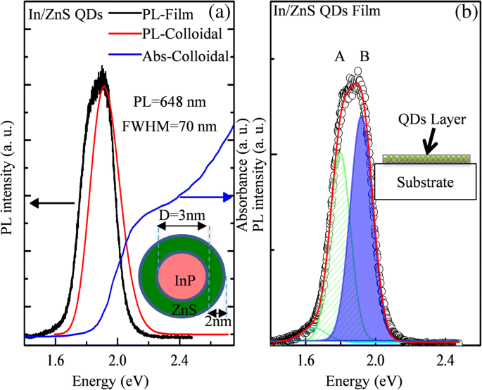
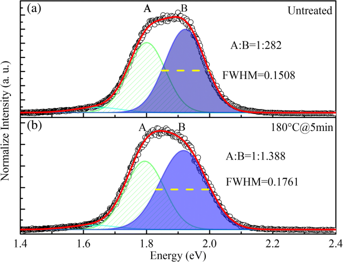
The colloidal QDs exhibit absorption at 2.215 eV (560 nm) and PL at 1.914 eV (648 nm) with a 70 nm FWHM. In the solid film, an additional low‑energy shoulder appears, attributed to QD clustering and localized states. Peak A (1.80 eV, 0.140 eV FWHM) and peak B (1.923 eV, 0.151 eV FWHM) were identified via Gaussian deconvolution.
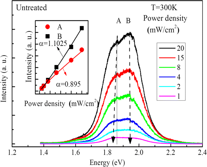
Power‑dependent PL (Fig. 2) revealed exponents α = 0.895 for peak A and α = 1.103 for peak B, confirming that peak A arises from localized states (α < 1) while peak B corresponds to band‑to‑band recombination (α ≈ 1). Peak A also exhibited a slight blue‑shift with increasing power, further supporting its localized‑state nature.
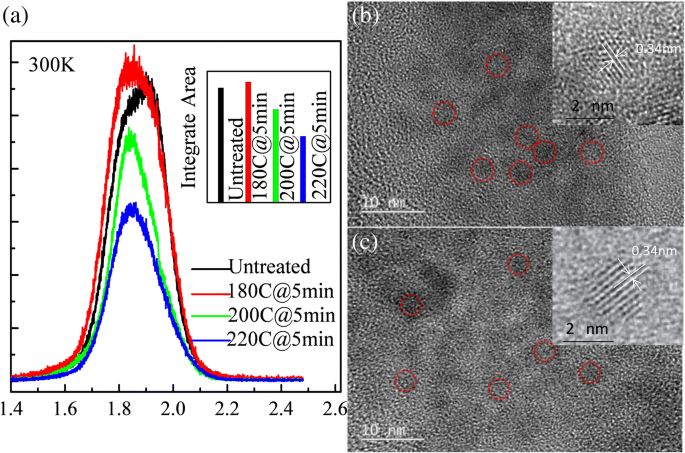
Four films were compared at 300 K (Fig. 3a). Annealing at 180 °C increased absolute PL intensity, whereas higher temperatures (200 °C, 220 °C) reduced emission due to the introduction of non‑radiative centers. TEM images (Fig. 3b,c) confirm that the crystalline structure and particle size (~3 nm) remain unchanged post‑annealing.
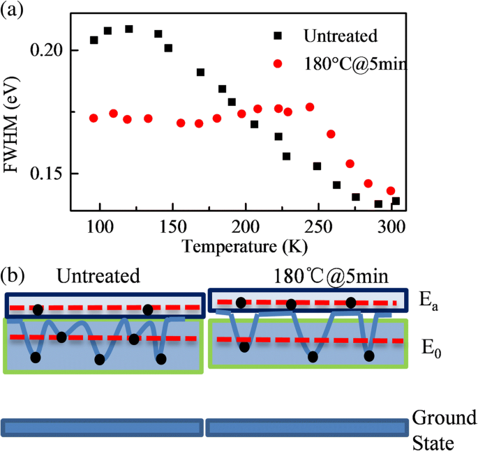
TDPL measurements (Fig. 4) tracked peak positions versus temperature. Peak B follows Varshni’s equation with parameters E_g(0) = 1.983 eV, α = 4.91 × 10⁻⁴ eV/K, β = 320 K for the untreated sample, and a slight 8 meV blue‑shift after annealing, indicating inter‑diffusion at the core‑shell interface. Peak A shows a red‑shift beyond 200 K, characteristic of carrier escape from shallow traps. After annealing, the depth of localization states increases, narrowing the FWHM at elevated temperatures (Fig. 6a). This behavior is captured by an energy‑band model (Fig. 6b) illustrating the redistribution of localized excitons.
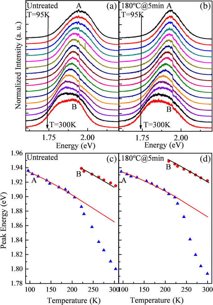
At 300 K, both films exhibit similar peak energies (A: 1.798 eV vs. 1.794 eV; B: 1.917 eV vs. 1.922 eV). However, the FWHM of peak B broadens from 0.1508 to 0.1761 eV after annealing, reflecting reduced inhomogeneous broadening.
FWHM versus temperature (Fig. 6a) shows that untreated films narrow with temperature, while annealed films maintain a constant FWHM up to 250 K before narrowing. This indicates that annealing removes shallow traps, leaving deeper localized states that persist until thermal activation.
Conclusions
Post‑thermal annealing at 180 °C for 5 min substantially improves the optical performance of InP/ZnS core/shell QD films. By combining temperature‑dependent peak shifts and power‑dependent PL exponents, we conclusively assign peak A to localized‑state emission and peak B to free‑carrier recombination. Annealing enhances free‑carrier emission by eliminating shallow traps, while deeper localized states remain. These insights inform the design of high‑efficiency QD‑based electroluminescent and down‑conversion devices.
Abbreviations
- FWHM
- Full width at half maximum
- PL
- Photoluminescence
- QDs
- Quantum dots
- QY
- Quantum yield
- RTA
- Rapid thermal annealing
- TDPL
- Temperature‑dependent photoluminescence
- TEM
- Transmission electron microscopy
Nanomaterials
- Eco-Friendly Synthesis of InP/ZnS Core/Shell Quantum Dots for High-Performance Heavy-Metal-Free LEDs
- Reversible Electrochemical Control of Photoluminescence in CdSe/ZnS Core/Shell Quantum Dot Films
- Aluminum‑Doped Zinc Oxide Thin Films: Infrared Optical Properties and Near‑Perfect Absorption Design
- High‑Performance Dual‑Emissive Mn‑Doped InP/ZnS Quantum Dots with 78 % Photoluminescence Quantum Yield: A Growth‑Doping Approach
- How Temperature Influences the Young’s Modulus of Electrospun Polyurethane Nanofibers
- Tailoring Optical Properties of InAs Quantum Dots with InAlAs Interlayers in GaAsSb Strain‑Reducing Layers
- Optimizing Niobium-Doped Titanium Oxide Layers for Enhanced Silicon Quantum Dot Solar Cells
- Enhanced Photon Absorption in Quantum Dot Infrared Photodetectors via Metal Nanohole Array Surface Plasmons
- Improving WLED Color Rendering with Composite Orange‑Red Quantum Dots
- Optical Performance of InGaN/GaN Quantum Wells: Effect of GaN Cap Layer Thickness