


Ethanol‑Driven Direct CVD Growth of High‑Quality Graphene on SiO₂ via an Intermediate Carbon Nanotube Stage
Abstract
Achieving high‑quality graphene on insulating substrates is pivotal for next‑generation graphene electronics. Here we report a catalyst‑free, atmospheric‑pressure chemical vapor deposition (APCVD) method that directly grows mono‑ to few‑layer graphene on SiO₂ using ethanol as a liquid hydrocarbon precursor. Systematic studies of annealing temperature and seed layers reveal that carbon atoms from thermal decomposition of ethanol nucleate as an sp² network, progressing through carbon nanoparticles and carbon nanotubes (CNTs) before forming continuous graphene films. This approach is compatible with standard silicon processing and extends to other dielectrics such as quartz, sapphire, and fused silica.
Introduction
Graphene on insulators is essential for electronic devices that avoid the metallic interference inherent to metal‑catalyst CVD. While vapor‑phase metal catalysts have enabled high‑quality graphene on SiO₂, direct catalyst‑free growth remains challenging and poorly understood. Recent advances have explored various dielectrics—h‑BN, glass, quartz, sapphire, Si₃N₄, SiO₂, and high‑k oxides—yet the resulting graphene often falls short of the quality achieved on metal foils or epitaxial SiC. Moreover, the growth mechanisms on insulators are still largely speculative.
Liquid hydrocarbon precursors, particularly ethanol, offer environmental, economic, and operational advantages over methane. Prior work demonstrated monolayer graphene on Cu from ethanol with a low I_D/I_G ratio (~0.04) at ~800 °C, suggesting ethanol’s potential to outperform methane on certain substrates. However, a comprehensive mechanism for ethanol‑driven graphene on insulators has not been established.
In this study, we introduce a novel APCVD protocol that directly deposits graphene on SiO₂ using ethanol, and we systematically investigate how annealing temperature and seed layers influence the growth process. The mechanism involves four stages: (1) vapor‑phase decomposition of ethanol; (2) graphitization on SiO₂ yielding carbon nanoparticles, CNTs, and intermediate structures; (3) hydrogen‑assisted etching that forms graphitic nanoribbons serving as nucleation sites; and (4) coalescence of nanoribbons into continuous high‑quality graphene after prolonged annealing.
Methods
Growth of Graphene on SiO₂
300‑nm SiO₂/Si wafers were cleaned with acetone and IPA, then sonicated and purged with N₂. In the APCVD chamber, substrates were heated to 1100 °C (10 °C/min) under 40 sccm H₂ and 250 sccm Ar. After a 5–10 min stabilization period, growth proceeded for 5–60 min with 10 sccm Ar carrying ethanol vapor (via a U‑shaped quartz tube). Samples were cooled to room temperature to yield continuous graphene films.
For seed‑assisted growth, substrates were pre‑coated with exfoliated graphene, charcoal, ECR‑CVD graphene, or CVD graphene, followed by 1‑h growth at 1100 °C under 4 sccm Ar.
Growth of ECR‑CVD Graphene for Seed Layer
SiO₂/Si wafers were cleaned and introduced into an ECR‑CVD chamber (vacuum 1×10⁻⁶ Torr). After surface cleaning with Ar plasma (5 sccm, 400 W, 5 min), the temperature was raised to 600 °C. Subsequently, Ar (5 sccm) and C₂H₄ (0.15 sccm) were introduced for 30 s at 1600 W, followed by 5 min annealing in 1 sccm H₂. The wafer was then cooled under vacuum.
Results and Discussion
CVD Growth of Graphene Using Ethanol
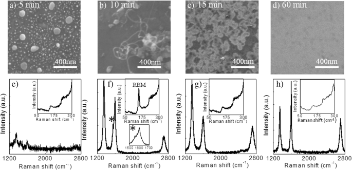
Figure 1 presents SEM images and Raman spectra of samples grown at 1100 °C for 5–60 min. Short growth (5 min) yields amorphous carbon nanoparticles (Raman D band prominent). After 10 min, CNTs emerge, evidenced by G‑band splitting (~1560 cm⁻¹) and a radial breathing mode near 150 cm⁻¹. At 15 min, CNTs transform into graphene islands with noticeable D‑band defects. Extended growth (60 min) results in nearly defect‑free, continuous graphene, as confirmed by a reduced I_D/I_G ratio.
Higher temperature growth (1150 °C) with reduced Ar flow (3 sccm) was also examined. SEM (Fig. 2) shows progressive nucleation: 2 h yields sparse flakes; 4–10 h increases density to mostly monolayer coverage (I₂D/I_G ≈ 1.5). Growth saturates after ~4 h, suggesting limited seed sites. While the yield (~80 %) is slightly lower than methane‑based CVD (~95 %), the catalyst‑free process eliminates post‑growth transfer.
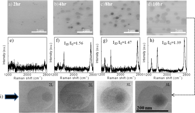
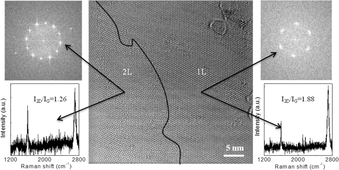
Figure 3 shows a TEM image of a 4‑h film: monolayer (I₂D/I_G = 1.88) and bilayer (I₂D/I_G = 1.26) regions coexist, with Moiré patterns indicating rotational misalignment.
Graphene Growth Mechanism on SiO₂
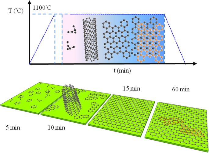
The mechanism (Fig. 4) starts with ethanol decomposition at ~700 °C:
C₂H₅OH(g) → C₂H₄(g) + H₂O. H₂ promotes further decomposition of ethylene to C and H atoms. Carbon atoms preferentially adsorb at SiO₂ step edges, forming disordered structures (5 min). With time, CNTs nucleate (10 min) as carbon arranges in spirals; continued growth (15–60 min) converts CNTs into sp² graphene islands that coalesce into continuous films. Hydrogen and water etch sp³ and amorphous carbon, leaving only sp² networks.
Seed‑Assisted Growth of Graphene
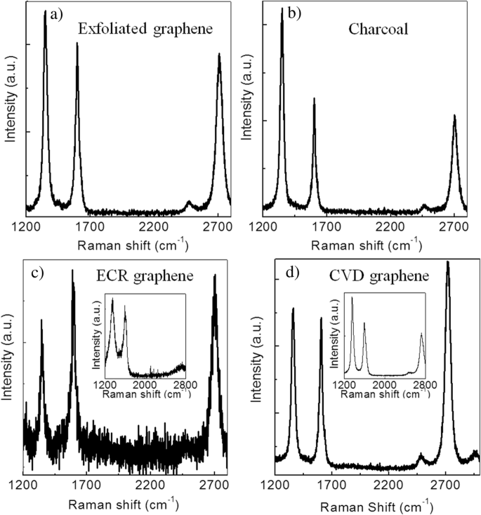
Four seed materials were evaluated: exfoliated graphene, charcoal, ECR‑CVD graphene, and CVD graphene (Fig. 5). Exfoliated and charcoal seeds yielded high‑defect graphene (large D band). ECR‑CVD seeds showed reduced D band but noisy spectra. CVD graphene seeds produced high‑quality, nearly single‑layer graphene (I₂D/I_G ≈ 1.35). XPS of 1‑h grown film (Fig. S4) shows a sharp C 1s peak at 284.4 eV (sp² C) with no extraneous elements, confirming the metal‑free synthesis.
Graphene Growth as a Function of Temperature
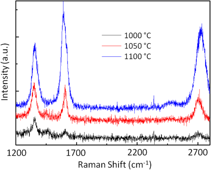
Growth at 1000 °C, 1050 °C, and 1100 °C (Ar/H₂ = 235:40 sccm, Ar = 10 sccm) was compared (Fig. 6). Lower temperatures produce broad 2D peaks, intense D bands, and multilayer, defect‑rich graphene. At 1100 °C, the 2D peak sharpens, indicating improved crystallinity, though some defects remain. Thus, 1100 °C is the optimum temperature for high‑quality, catalyst‑free graphene on SiO₂.
Validation with CNT Precursors
To confirm the intermediate CNT role, CNTs were deposited on SiO₂ before CVD. Raman mapping (Fig. S5) shows CNTs transforming into graphene after 10 min, with diminishing RBM and D peaks and increasing 2D/G ratio.
Conclusions
We have established a catalyst‑free APCVD process that uses ethanol to grow mono‑ to few‑layer graphene directly on SiO₂. The growth proceeds through an intermediate CNT state, with hydrogen and water selectively etching amorphous carbon to leave a pristine sp² network. Growth temperature and seed layers critically affect crystallinity; 1100 °C and CVD graphene seeds yield the best results. This method aligns with standard silicon fabrication, obviating metal catalysts and transfer steps, and paves the way for graphene integration in silicon‑based electronics.
Abbreviations
- AFM
- Atomic force microscopy
- CNTs
- Carbon nanotubes
- CVD
- Chemical vapor deposition
- ECR‑CVD
- Electron cyclotron resonance‑CVD
- FWHM
- Full width at half maximum
- MLG
- Multilayer graphene
- PMMA
- Polymethyl methacrylate
- RBM
- Radial breathing mode
- SEM
- Scanning electron microscopy
- SWCNT
- Single‑wall carbon nanotube
- TEM
- Transmission electron microscopy
- XPS
- X‑ray photoelectron spectroscopy
Nanomaterials
- Carbon Nanotube Yarns, Artificial Muscles, and Transparent Sheets: Advanced Applications
- Direct Growth of III‑Nitride Nanowire LEDs on Amorphous Quartz Using a TiN/Ti Interlayer
- Spherical Graphene/SiO₂ Supports Enable Uniform In Situ Polymerization of UHMWPE for High‑Performance Nanocomposites
- Electrochemical Energy Storage: Enhancing Capacitance with Reduced Graphene Oxide/Carbon Nanotube Composites
- Optimizing Vertically Aligned Carbon Nanotube Growth: The Key Role of Oxide Buffer Layers in CVD
- Angle‑Insensitive Broadband Graphene Absorber Enabled by a Multi‑Groove Metasurface
- Efficient Large-Area Single-Layer Graphene on Copper via Refined Palm Oil and Spray-Injector CVD
- Optimizing Buffer Layers via Atomic Layer Deposition for High‑Performance Vertically Aligned Carbon Nanotube Arrays
- Advances in Carbon Nanotube Assembly and Integration for Next‑Generation Applications
- Controlled Low‑Temperature Growth of WSe₂ on Graphene for Efficient p‑Type Transistors