


Semiconductor Manufacturing Techniques: From Silicon Purification to Integrated Circuit Fabrication
The following overview focuses exclusively on silicon-based semiconductor fabrication, the predominant material in modern integrated circuits. Silicon’s unique ability to form a stable oxide layer makes it ideal for precise patterning of transistors and other microcomponents.
Silicon
Silicon is the second most abundant element in the Earth’s crust, primarily as silicon dioxide (SiO2)—commonly known as silica sand. Industrially, silicon is extracted by reducing SiO2 with carbon in an electric‑arc furnace:
SiO2 + C → CO2 + Si
The resulting metallurgical‑grade silicon is suitable for applications such as transformer laminations but falls short of the purity required for semiconductor devices. To achieve semiconductor‑grade purity, the silicon is first converted into a chloride—SiCl4 or SiHCl3—which can be purified by fractional distillation. Subsequent reduction with ultrapure zinc or magnesium yields a “sponge” form of silicon, which is then refined further. Thermal decomposition of SiHCl3 on a heated polycrystalline silicon rod using hydrogen gas is another route to ultra‑pure silicon.
Si + 3HCl → SiHCl3 + H2
SiHCl3 + H2 → Si + 3HCl2
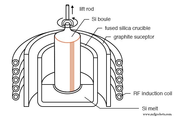
Once purified, the polycrystalline silicon is melted in a fused‑silica crucible, heated via an induction‑heated graphite susceptor or a direct‑current high‑current heater. The Czochralski process then draws a monocrystalline “boule” from the melt, maintaining crystal lattice orientation and controlled diameter. Dopants such as phosphorus or boron are introduced into the melt to engineer p‑type or n‑type conductivity. The entire growth chamber operates under an inert atmosphere to prevent contamination.
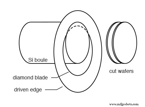
The boule is ground to a precise diameter and trimmed at the ends. It is then sliced into wafers using a diamond‑tipped saw. Subsequent grinding and polishing yield wafers with sub‑micron surface roughness. An optional epitaxial n‑type layer can be thermally deposited atop the wafer to further enhance device performance. These wafers are then shipped to semiconductor fabs for device fabrication.
Processing of Semiconductors
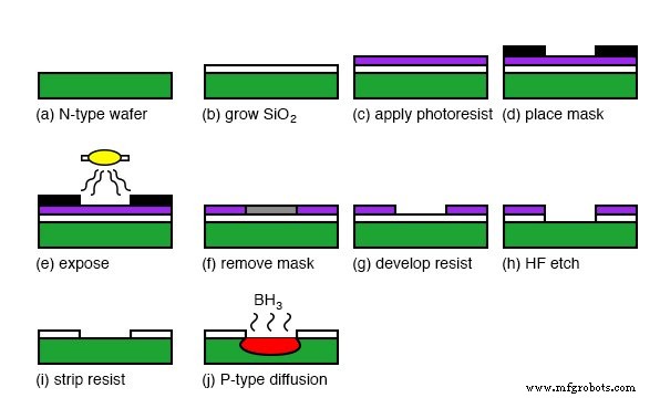
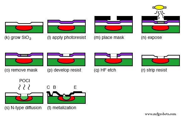
Photolithography is the cornerstone of semiconductor patterning. The process parallels that used for copper printed circuit board (PCB) fabrication, albeit with higher temperatures and tighter tolerances. The steps are:
- Apply a positive photoresist to the wafer surface.
- Spin the wafer to evenly spread the resist.
- Expose the resist through a chrome‑on‑glass mask under ultraviolet light.
- Develop the exposed resist in an alkaline solution, removing the softened regions.
- Etch the wafer—usually with hydrofluoric acid (HF) to open windows in the protective silicon dioxide layer.
- Strip the remaining resist and subject the wafer to high‑temperature diffusion.
Hydrofluoric acid selectively removes silicon dioxide while leaving silicon untouched, creating precise windows for dopant diffusion. Dopants are introduced in gaseous form (e.g., POCl3 for n‑type or B2O3 for p‑type) within a diffusion furnace operating above 1000 °C. Diffusion only occurs through the windows, forming well‑defined PN junctions.
Following dopant diffusion, metallization steps create electrical contacts. Photolithography is repeated to pattern metal layers (often aluminum or copper) that interconnect multiple transistors into integrated circuits. Finally, the wafer is diced into individual dies, wire‑bonded to a lead frame, and encapsulated into packages.
Key Takeaways
- Ultra‑pure silicon is essential for creating the glassy SiO2 layer that serves as the photolithographic resist.
- The Czochralski method produces single‑crystal silicon boules that are diamond‑sawed into wafers.
- Photolithography on silicon mirrors PCB fabrication, using photoresist, UV exposure, development, HF etching, and dopant diffusion.
- Controlled diffusion of gaseous dopants at high temperatures forms the active regions of diodes and transistors.
- Repeated lithography and metallization steps enable the integration of thousands of devices on a single wafer.
Related Resources
- Printed Circuit Board Layout and Manufacture Worksheet
Industrial Technology
- Expert Guide to JFET Biasing Techniques: Achieve Stable, High‑Performance Circuits
- Wally Rhines Projects Silicon Transistor Growth Through 2038
- Practical Design Strategies for Additive Manufacturing and Rapid Prototyping
- Reducing the Environmental Footprint of Semiconductor and Electronics Production
- 20+ Fusion 360 Additive Manufacturing Techniques & Comprehensive Tutorials
- Proven Manufacturing Techniques for Printed Prototype Circuit Boards
- Semiconductor Manufacturing: The Critical Role of Rapid Support Services
- Semiconductor Evolution Unveiled: Past, Present, and Future – Expert Q&A
- Overcoming Key Challenges in ALD and ALE Semiconductor Processing
- Next-Gen Semiconductor Manufacturing: Innovating for the Digital Future