


Cadence Launches ML‑Driven Cerebrus Tool to Boost Chip Design Productivity by 10× and PPA by 20%
Chip design is rapidly evolving—customers demand more features, smaller footprints, and lower power, driving complexity to new heights. Engineers are increasingly stretched thin, making it difficult to deliver products on schedule. Cadence Design Systems responds with Cerebrus Intelligent Chip Explorer, a machine‑learning (ML)–powered tool that optimizes the entire RTL‑to‑signoff flow.
Cerebrus claims up to a 10‑fold increase in design productivity and a 20% improvement in power, performance, and area (PPA) across a wide range of applications, from consumer electronics to hyperscale computing, 5G, automotive, and mobile design. The solution combines on‑site and cloud compute to automate what traditionally required dozens of engineers and months of manual iteration.
“This is the first full‑flow digital optimization tool using ML,” said Rod Metcalfe, Cadence’s product‑management group director. “As design complexity grows, engineers are forced to iterate manually, which is not scalable. Cerebrus leverages massive compute to streamline automation and unlock higher productivity.”
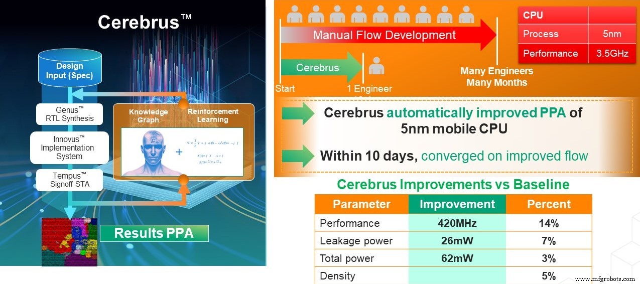
Metcalfe highlighted a case where a single engineer converged on an improved 5 nm mobile CPU design in just 10 days, automatically boosting its PPA.
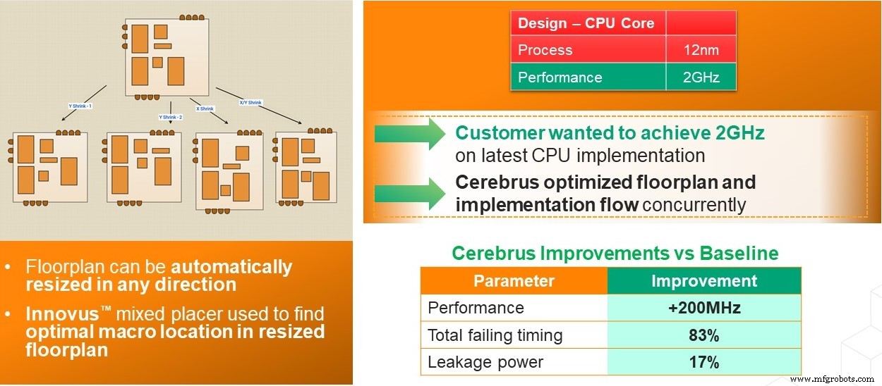
Another use case demonstrates automated floorplan optimization, yielding significant timing and power gains.
By reusing historical design knowledge, Cerebrus eliminates repetitive manual learning, freeing engineers to focus on high‑impact tasks. Cadence describes this as a “revolution” in electronic design automation (EDA), positioning the tool as essential for teams tackling advanced nodes and ever‑increasing design complexity.
Early adopters include Renesas and Samsung Foundry. Renesas’s Satoshi Shibatani noted that automated flow optimization with Cerebrus delivered over 10% improvement in design performance. Samsung Foundry’s Sangyun Kim reported more than 8% power reduction on critical blocks and a 50% improvement in timing after just a few days of use.
- Reinforcement ML: Explores non‑obvious flow solutions, enhancing PPA and productivity.
- ML model reuse: Applies past learnings automatically to new projects, shortening the learning curve.
- Improved productivity: A single engineer can auto‑optimize full RTL‑to‑GDS flows for multiple blocks concurrently.
- Massively distributed computing: Scales on‑premises or cloud resources for rapid exploration.
- Intuitive interface: Interactive cockpit provides real‑time analytics and run management.
Cerebrus integrates seamlessly with Cadence’s broader digital full‑flow suite—including Genus synthesis, Innovus implementation, Tempus timing signoff, Joules RTL power, Voltus IC power integrity, and Pegasus verification—offering customers a fast, predictable path to design closure.
Embedded
- QuickLogic Launches Australis: Automated eFPGA IP Generator for Rapid, Custom ASIC Prototyping
- Accelerating CPU‑FPGA Co‑Design: A Practical Flow for Software Developers
- Intel Launches Loihi 2: Next‑Gen Neuromorphic Chip with Advanced Programmability and 3D Scaling
- Eta Compute Strengthens AI Ecosystem with New Compiler, Sensor Board, and Edge Impulse Partnership
- Designing Multi‑Antenna PCB Layouts: Best Practices for Co‑existence and Isolation
- Comprehensive ASIC Design Flow: From Requirements to Production
- Pennsylvania Allocates $110,000 to Expand Manufacturing Careers for Philadelphia Students
- MS52 CNC Bar/Chucker: Open‑Front Design for High‑Volume Production
- Purdue Engineers Develop Hidden Transistor Design to Shield Chips from Reverse Engineering
- Vericut 8.1 Unveils Advanced AM Module for Precise Simulation, Verification & Optimization