


Optimizing Size, Power, and Cost in Infrared Thermal Imaging Systems
Thermal imaging spans industrial manufacturing, security, and environmental monitoring. Because infrared wavelengths differ from visible light, designers must tailor hardware for optimal performance—resulting in smaller, lower‑power, and more cost‑effective systems.
The Infrared Spectrum
The human eye captures only the visible portion of the electromagnetic spectrum. Infrared (IR) radiation lies beyond visible light and is the key to detecting heat signatures—an object's temperature directly dictates its IR output.
Originally used for night‑time target acquisition, thermal cameras now serve a broad range of purposes, including:
- Early fire detection and plant health monitoring
- Factory automation and Industry 4.0 processes
- Energy audits that locate heat leaks in buildings
- Night‑time perimeter and wildlife surveillance
- Storm and hurricane tracking
- Medical diagnostics of temperature anomalies
- Inspection of aircraft, trains, and other heavy equipment
- Wildlife conservation and precision agriculture
- Disaster response and rescue operations
The growing list of applications drives continued R&D investment, making thermal cameras increasingly powerful and affordable.
A typical thermal camera consists of a housing, lens, IR sensor, and on‑board electronics—image processor, FPGA, memory, communication, and display circuits. The lens concentrates IR energy onto the sensor, which converts the heat signature into a visible image.
IR sensors are available from 80 × 60 up to 1280 × 1024 pixels. Compared to visible‑light cameras, each pixel must be larger (≈ 25 µm versus 1.7 µm in consumer sensors) to capture the longer wavelengths. Consequently, thermal cameras have lower overall resolution, but the larger pixel size allows precise temperature measurement—some models detect differences as small as 0.01 °C.
Memory Challenges
The FPGA in a thermal camera processes raw sensor data. Its internal RAM is often insufficient, so designers rely on off‑chip memory for algorithms, display buffering, and communication. Off‑chip storage also provides scalability for future density increases.
Traditionally, DDR DRAM is used for this purpose. However, the modest resolution of thermal images means that high‑density DRAM is unnecessary, adding cost, extra pins, and power draw. DRAM’s volatility requires periodic refresh, further increasing consumption—an issue for battery‑powered devices.
Infineon’s HyperRAM addresses these limitations. Built on a DRAM core with built‑in self‑refresh, HyperRAM draws only 25 mA, dramatically reducing power while delivering comparable throughput (≈ 400 MB/s). It uses a 12‑pin HyperBus interface, far fewer than DDR’s 30+ pins, simplifying PCB routing and layer count.
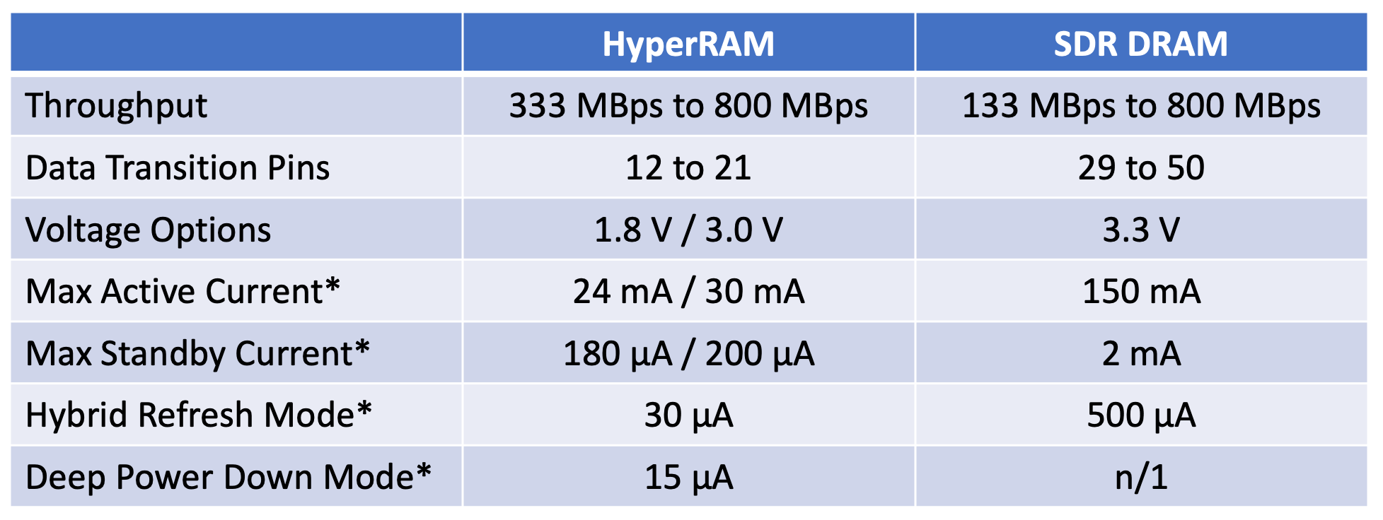
Table: HyperRAM vs SDR DRAM (64 Mb device). Source: Infineon Technologies
The HyperBus Memory Controller can be implemented as soft IP in the FPGA, eliminating the need for a bulky DDR controller. Figure 1 shows the pin‑count advantage: a DDR‑based system requires two buses totaling 41 pins and six PCB layers, whereas a HyperRAM/HyperFlash system uses a single 13‑pin bus and only two to four layers.
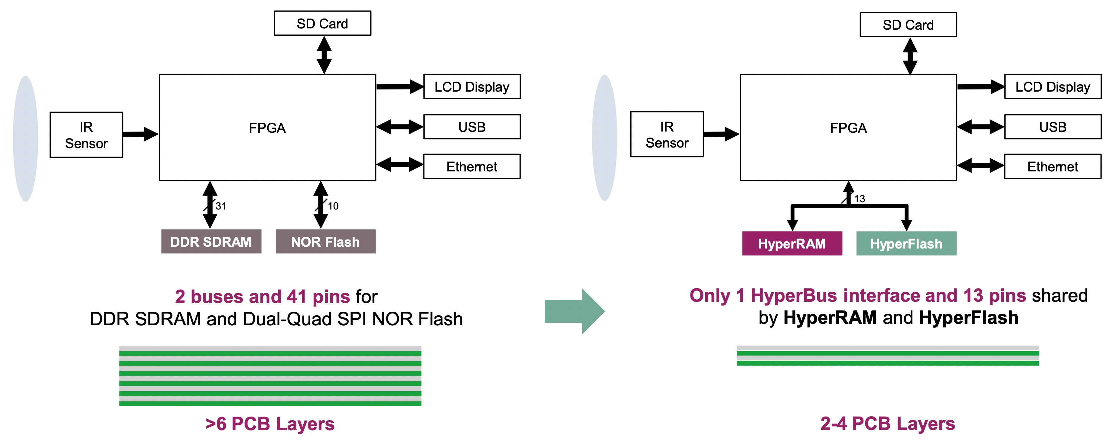
Figure 1: Pin‑count comparison between DDR‑SDRAM/NOR Flash and HyperRAM/HyperFlash. Source: Infineon Technologies
External NOR Flash is also common for non‑volatile configuration storage. HyperFlash—NOR Flash with the HyperBus interface—can share the same 13‑pin bus as HyperRAM, reducing pin count from 41+ to just 13. HyperFlash and HyperRAM are available in 64–512 Mb densities, with HyperBus and Octal xSPI JEDEC‑compliant interfaces.
By selecting memory that matches thermal imaging requirements, OEMs can streamline PCB design, lower cost, cut power consumption, and extend battery life.
 Bobby John is Senior Product Marketing Manager in the Memory Solutions business at Infineon Technologies and has over 13 years of experience across various roles in the Semiconductor Industry.
Related Contents:
- Sensors and processors converge for industrial applications
- How serial Flash technology is evolving to meet the new requirements of Industry 4.0 designs
- Why FIR sensing technology is essential for achieving fully autonomous vehicles
- Sensor systems in the industrial IoT
- New ams image sensors for high throughput industrial vision
For more Embedded, subscribe to Embedded’s weekly email newsletter.
Embedded
- Transformers: Advanced Impedance Matching & Specialized Applications
- Future Electronics Launches Rapid‑Development Arduino‑Compatible Thermal Imaging & IR Sensing Platform
- Maxim Integrated’s New Sensors Slash Power, Size, and Boost Accuracy for Wearable Health Devices
- Maxim Integrated Launches Three Low‑Power Analog ICs to Drive Efficiency in Edge and Cloud Applications
- Bluetooth 5.1 SoC: Ultra‑Compact, Low‑Cost Solution for IoT Devices
- u‑blox Launches SARA‑R5 LTE‑M/NB‑IoT Modules: 5G‑Ready, Ultra‑Secure, Low‑Power for Long‑Term IoT Deployments
- Designing Robust Circuit Protection, Control, and Sensing for Smart Home Security Systems
- Magnetic Core‑Shell Nanoparticles: Advancing Targeted Drug Delivery, Imaging, and Antimicrobial Therapies
- Six-Axis Industrial Robots: Real-World Uses, Benefits, and Cost Breakdown
- Variable Speed Drives: Keeping Food, Medicine & More Cool in Industrial Refrigeration