


Why Antenna Placement Matters: Redesigning the Wireless PCB Lifecycle
The integration of a wireless antenna fundamentally changes the PCB design cycle. Antennas demand meticulous positioning, thoughtful clearance from nearby components, and a deep understanding of the RF environment to achieve reliable performance.
Before you lay out the rest of the board, map out the RF pathway: select the antenna, determine its optimal placement, define the ground plane, and plan short, low‑loss transmission lines. Each step adds layers of complexity, but mastering them ensures your product meets both performance and regulatory expectations.
Antenna Selection
Embedded antennas are the industry standard, offering excellent performance in minimal space. Surface‑mounted device (SMD) antennas are typically 1 mm across, fabricated on high‑grade dielectric substrates, and reflowed directly onto the PCB during assembly.
For designers who need a plug‑and‑play solution, ready‑made antenna modules combine the antenna with RF circuitry, simplifying integration.
When board real estate is scarce, flexible printed circuit (FPC) antennas shine. Their copper tape layer and integral UFL connector allow the antenna to conform to tight corners or curved surfaces, making them ideal for handheld gadgets.
If your design incorporates metal components that could detune an embedded antenna, consider an external option. External antennas—whether terminal, PCB‑mounted, or case‑mounted—are insulated from nearby metal, deliver consistent performance, and free valuable PCB area for other components.
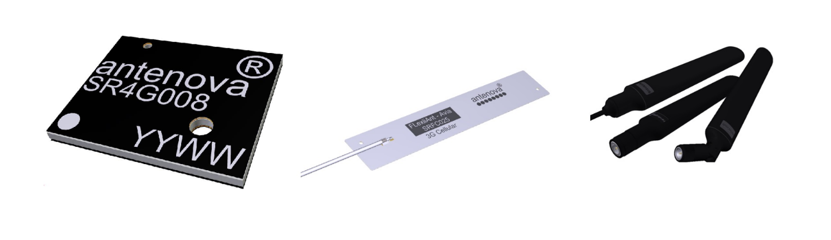
Figure 1. External antenna options include (left to right) an SMD antenna, an FPC antenna, or terminal antennas. Source: Antenova
Antenna Placement
Placement is critical. The antenna radiates primarily along its length, so it should have maximum free space on all sides. Manufacturers specify optimal mounting locations in the datasheet, but a common strategy is to place the SMD antenna on the PCB corner or edge.
Keep these components away: motors, batteries, and high‑metal content elements like LCDs can introduce noise and impedance mismatches.
Even the device enclosure matters. Plastic casings, with a higher dielectric constant than air, can detune the resonant frequency; a careful study of enclosure materials is advisable.
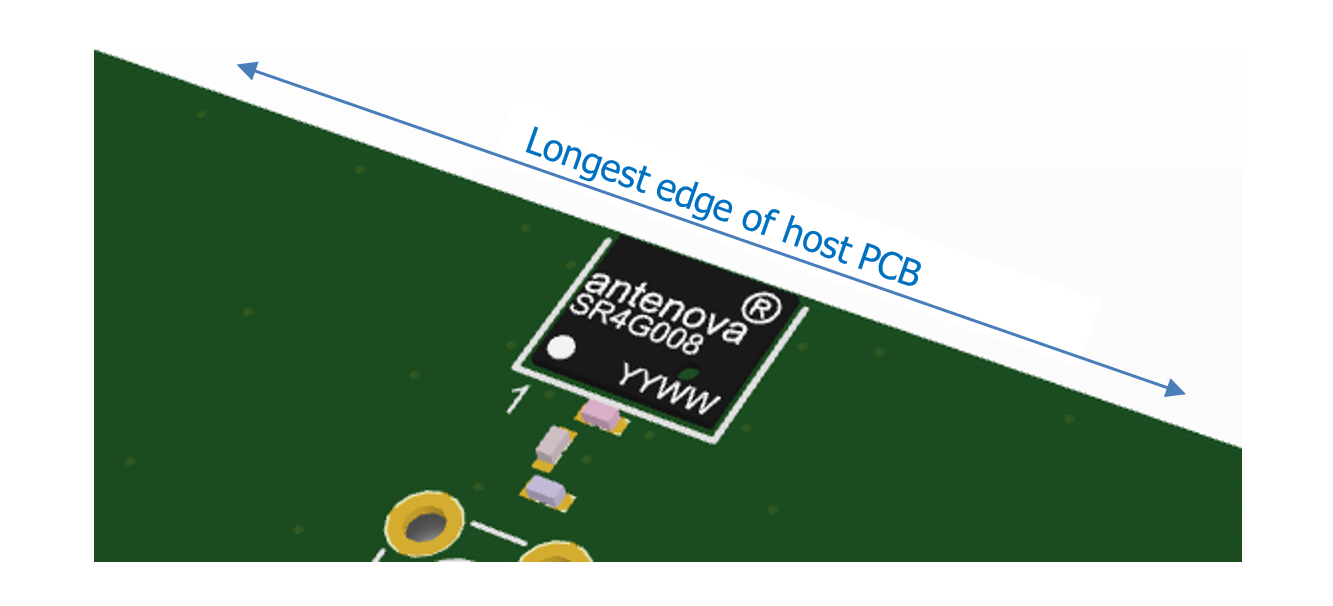
Figure 2. An SMD antenna is placed on the long edge of a PCB. Source: Antenova
Ground Planes and RF Board Design
Effective radiation requires a contiguous ground plane. The plane’s size is related to the longest wavelength of the antenna; datasheets will specify the exact dimensions.
Maintain a clear keep‑out area around the antenna—often several layers—free from other components. Short RF traces minimize reflections and power loss; place the radio as close to the antenna as possible.
For narrow bandwidth antennas or constrained board space, a lumped element matching network (e.g., a Pi network) can boost bandwidth and overall performance.
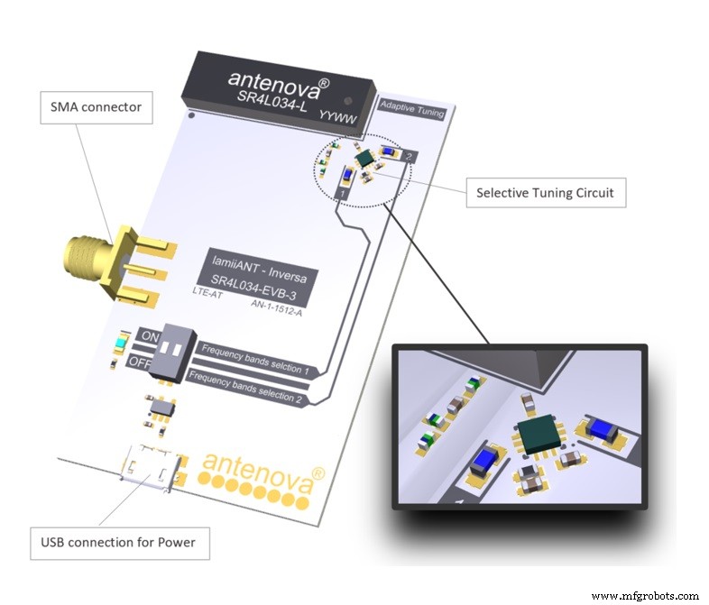
Figure 3. An antenna design with an active tuning circuit can overcome the bandwidth reduction seen with a smaller ground plane. Source: Antenova
Gerber Review and RF Testing
A Gerber file review is essential before finalizing the layout. It verifies antenna placement, trace geometry, via placement, and PCB material selection to ensure optimal RF performance. Many antenna vendors offer this review free of charge, or you can use dedicated design software.
Real‑world performance must be validated in an anechoic chamber. For devices that will operate near the human body or in cluttered environments, test with a phantom head or hand to capture realistic interactions.
Further assessments—passive, over‑the‑air (OTA), and synthetic aperture radar (SAR) tests—evaluate efficiency, spurious emissions, radiated power, and isotropic sensitivity, ensuring compliance with regulatory standards.
Finally, all cellular devices must obtain carrier network certification before commercial deployment.
>> This article was originally published on our sister site, EDN.
 Geoff Schulteis is an RF antenna application specialist and leads technical support for Antenova’s North American customer designs.
Related Contents:
- Integrating chip antennas into a PCB: Understanding antenna matching
- How to get better wireless performance for mobile devices with small PCBs
- Addressing PCB design concerns
- Transforming chip and system communications
- How system level noise in digital interfaces can lead to spurious errors in serial Flash memory
For more Embedded, subscribe to Embedded’s weekly email newsletter.
Embedded
- Embedded System Design: Steps, Principles, and Real‑World Applications
- Designing Multi‑Antenna PCB Layouts: Best Practices for Co‑existence and Isolation
- Designing an Effective Maintenance Strategy: A Practical Roadmap
- Understanding the Metal FFF 3D Printing Process: From Printing to Sintering
- Secure Remote Access: Driving Innovation in Process Industries
- Accelerate Innovation: Harnessing Engineering Design to Speed Up Product Development
- Inside GE Aviation’s CMC Production: From Silicon Carbide to Composite Parts
- Mastering Polyurethane Production: Process Insights & Cost‑Saving Strategies
- Industry 4.0 in Process Industries: Proven Steps to Boost Efficiency and Innovation
- Maximizing CAD Efficiency in Additive Manufacturing