


Mastering Multiprotocol Miniature Wireless Integration: Design & Implementation Guide
Designing a multiprotocol wireless system typically follows one of two paths: building from scratch with a dedicated RF chip, passive components, filters, and an antenna; or selecting an off‑the‑shelf wireless module that already integrates these elements.
Build from scratch or use a module?The primary benefit of a custom build is a lower unit cost at very high volumes. However, to achieve a cost advantage across the entire project lifecycle—design, testing, certification, procurement, and manufacturing complexity—massive volume production is usually required.
Module advantagesBecause modules bring together pre‑integrated components that are typically certified for the major markets, many designers opt for them. Modules shorten design time, reduce cost, and often offer a smaller footprint than a comparable discrete implementation.
Wireless solutions are increasingly sophisticated, diverse, and capable. In many applications a single radio technology is insufficient, creating the need to integrate multiple radios while ensuring they do not interfere. RF systems can exhibit complex, non‑obvious interactions.
Multiple radios in a single deviceAdding more than one certified radio also escalates certification complexity: each modular radio may require additional testing when combined into a single unit.
Pre‑packaged multiprotocol solutionsTo address this, a growing trend is the availability of pre‑packaged multiprotocol wireless modules. Combined Bluetooth and Wi‑Fi modules have been common for some time; because they share the 2.4 GHz band, they can often share a single antenna.
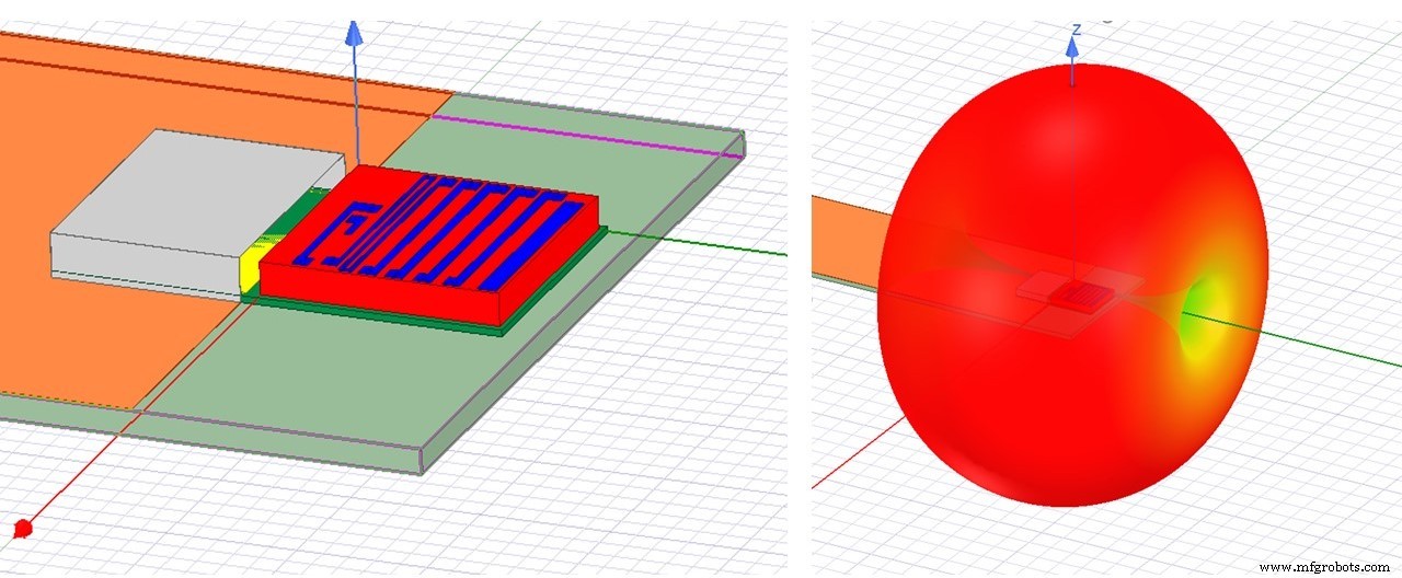
Integrating different radios – case studyAs an example, we examined the integration of a 2.4 GHz Bluetooth Low Energy device with a sub‑gigahertz LoRa radio. The challenge was to fit the electronics and both antennas into the smallest package possible.
First step – module electronicsThe design began with a system‑in‑package (SiP) architecture, targeting a 200 µm inter‑layer spacing. Such tight spacing heightens the risk of RF crosstalk and interference, so a rigorous design cycle was essential.
An initial layout was generated using hard design rules and industry best practice. To avoid endless prototype manufacturing, an iterative simulation‑driven approach was adopted. A 3‑D PCB model was simulated in Ansys HFSS (equivalently CST or ADS FEM). Because third‑party components rarely provide full physical models, N‑port S‑parameter models were used instead, offering a close approximation of RF performance.
With a complete RF simulation, key performance metrics—return loss, harmonic content, and out‑of‑band emissions—could be evaluated. This enabled optimisation for the target frequency bands and ensured compliance with regulatory limits before any physical prototype was built.
Second step – antenna designThe antenna subsystem presented two main challenges:
- Creating a miniature antenna for sub‑gigahertz operation.
- Ensuring coexistence of the two antenna functions.
The LoRa radio operates between 868 MHz and 930 MHz, depending on the country, which corresponds to a 32 cm wavelength. Achieving a quarter‑wave length in a device limited to 2 cm is therefore a significant engineering hurdle.
The 2.4 GHz antenna, while easier to miniaturise, has distinct physical requirements compared to the sub‑gig antenna.
Two design strategies were evaluated: (1) separate antennas within the same device, and (2) a single multimode antenna with a diplexer to route the two radios. Each option was explored in three physical configurations—simple trace on the substrate, a 3‑D structure using vertical vias through the SiP overmold, and a dedicated 3‑D antenna component embedded in the overmold.
An iterative approachLike the electronics, the antenna design followed an iterative process that combined design expertise, 3‑D electromagnetic simulation, and successive optimisation cycles. Several topologies were initially considered and then refined to a final solution.
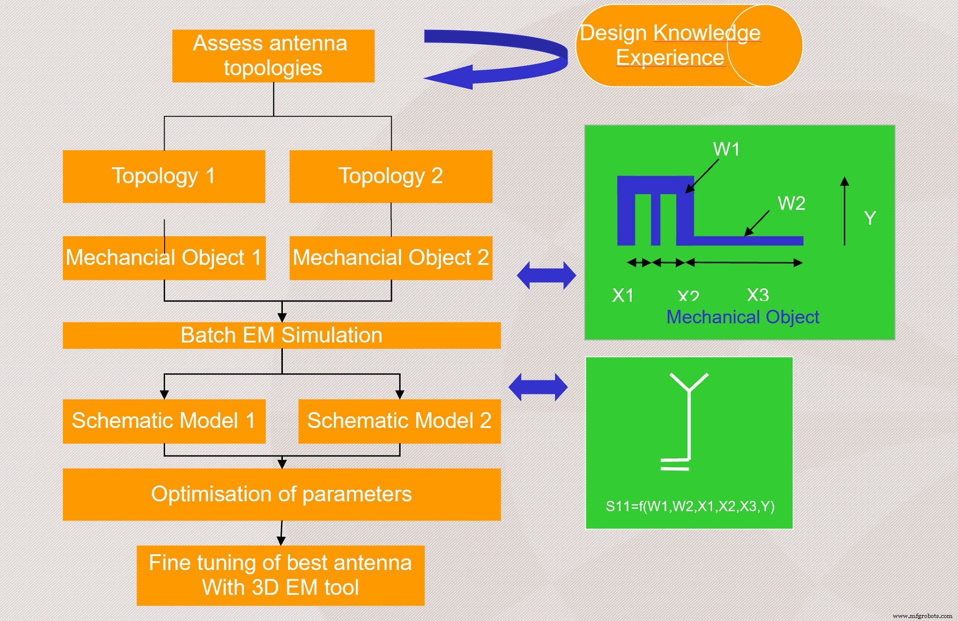
Three‑dimensional simulation is indispensable; the cost of designing, fabricating, and testing physical antennas would be prohibitive and likely yield sub‑optimal results. Once a simulation‑optimised design is produced, a prototype is fabricated and measured. The measured data is then fed back into the model, refining the simulation and accelerating convergence. In practice, only two build‑test cycles are usually required to achieve a final design.
RF engineering is often called “black magic,” but it simply follows the same physical laws that govern all electronics. The complexity lies in translating a schematic into a physical layout without compromising performance; unlike digital logic, RF topologies are highly sensitive to trace geometry and parasitics.
Create the full solutionThe final solution is the result of deep expertise, up‑to‑date simulation tools, and iterative optimisation. A strong starting point, informed by industry experience, combined with rapid simulation cycles, allows designers to achieve first‑time success or, at worst, a second‑time redesign.


Related Contents:
- Cutting the complexity of wireless connectivity, co‑existence
- Untangling in‑vehicle wireless power design challenges
- Sierra Wireless divests automotive embedded modules to Fibocom Wireless
- Which wireless technology will win the lightweight WAN battle?
- How to get better wireless performance for mobile devices with small PCBs
Embedded
- Consumer Product Design: A Practical Guide for Success
- Design for Manufacturability: A Practical Guide for Engineers and Designers
- Arrow Electronics Launches Power‑Efficient Sharky IoT Wireless Modules
- Why Antenna Placement Matters: Redesigning the Wireless PCB Lifecycle
- Mastering Multiprotocol Miniature Wireless Integration: Design & Implementation Guide
- Designing Multi‑Antenna PCB Layouts: Best Practices for Co‑existence and Isolation
- Expert Guide to Saudi Arabian Furniture Design Trends and Market Insights
- Flexible Wireless Transmitter for Wearable Medical Sensors
- Chip vs. PCB Antennas: Choosing the Optimal RF Solution for Embedded Designs
- Optimizing Antenna Design for Compact IoT Devices