


Optimizing Wireless Performance on Tiny PCBs for Mobile Devices
The demand for smaller wireless devices is rising across consumer markets—wearables, medical gadgets, trackers—and industrial sectors such as lighting, security, and building management. As product footprints shrink, the PCBs that host their antennas become smaller, forcing designers to work with reduced ground planes and tighter power budgets for battery‑operated devices.
Meeting this challenge is critical because every final design must undergo formal network and government certification before it can operate on carrier networks. A sub‑optimal antenna can fail certification, re‑radiate device noise, or produce interference that jeopardises transmit and receive thresholds—especially stringent in the United States, where regulatory bodies demand precise performance metrics.
Electrically small antennas operating below 1 GHz ideally require ground‑plane lengths of 100 mm or more to achieve acceptable efficiency. Shorter ground planes degrade efficiency, driving higher power consumption and making it difficult to satisfy network approval. Consequently, designers must carve out enough space for a robust ground plane while still accommodating all components on a miniature PCB.
This rule of thumb applies to the common IoT, tracker, and fitness devices that typically operate below 1 GHz.
Wearable and medical devices pose an extra hurdle because the human body attenuates RF signals. Antenna placement must minimise body‑blocking effects, which means careful consideration of orientation and distance from the body.
Some wearables are as compact as 50 mm, and certain products even host multiple antennas.
Several factors influence antenna performance in a small device. Ground‑plane size is paramount, but designers also need to position the antenna correctly, avoid nearby noisy or metallic components, and choose a suitable enclosure material.
Embedded Antennas – How They Work
An embedded chip antenna uses a single radiator; the PCB surface acts as the second arm of the dipole. If the PCB is too short, the antenna cannot resonate efficiently.
Resonance is tied to wavelength: a quarter‑wave monopole at 916 MHz requires a ground plane of roughly 87 mm—practical for surface‑mounted designs. Designers often treat the ground plane as the missing half‑wave dipole, making quarter‑wave monopoles the most popular choice for compact devices.
Ground‑Plane Length
For optimal efficiency, the ground plane should be at least a quarter of the operating wavelength. At frequencies below 1 GHz, this translates to a ground‑plane length of 100 mm or more.
Figure 1 illustrates how efficiency drops sharply when the ground plane is shortened, across bands from 794 MHz to 2.69 GHz.
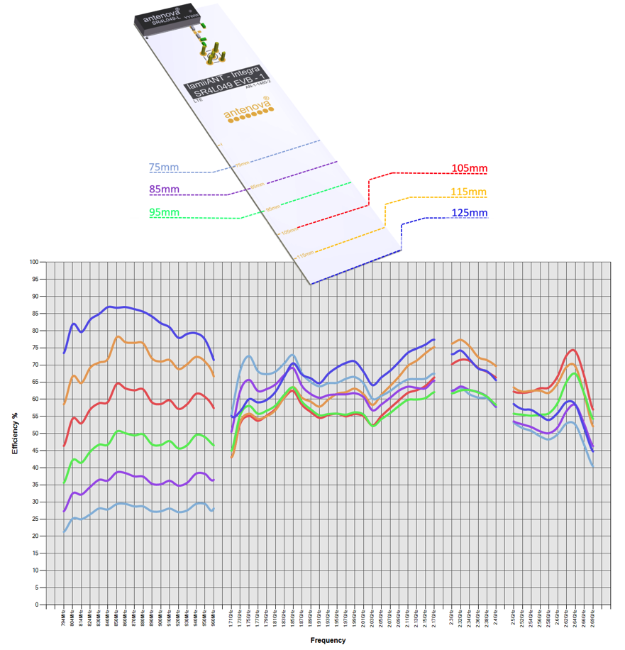 Figure 1. (Source: Antenova Ltd)
These measurements come from a 3G/4G chip antenna covering 791–960 MHz, 1710–2170 MHz, 2300–1400 MHz, and 2500–2969 MHz. For sub‑1 GHz operation, a 100 mm ground plane is typically required. In the U.S., 4G bands such as 698 MHz or T‑Mobile’s B71 at 617 MHz demand even longer ground planes.
Positioning the Antenna on Its PCB
Placement within the RF layout and PCB stack‑up is critical. Many antennas perform best at corners or edges, but specific recommendations depend on the manufacturer’s datasheet.
Figure 2 shows an example of clearance around an antenna on a wearable or watch PCB.
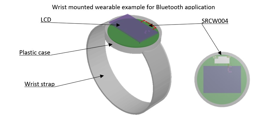 Figure 2. (Source: Antenova Ltd)
Figure 3 demonstrates a suitable placement for a watch, respecting the required clearance zones marked in red.
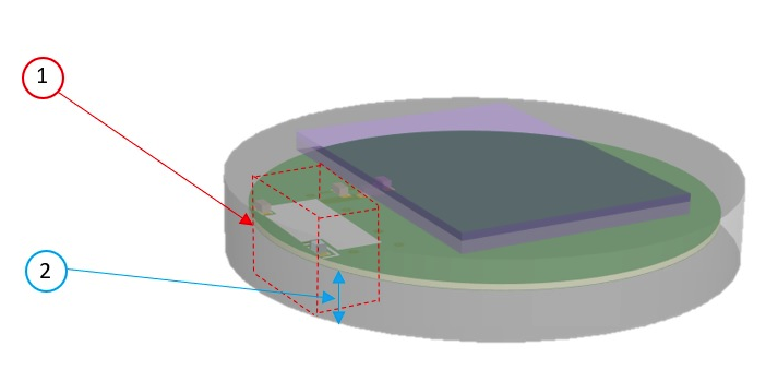 Figure 3. (Source: Antenova Ltd)
Avoid positioning noisy components—batteries, LCDs—near the antenna. Noise coupled into the antenna degrades the received signal. Keep the antenna away from the body; the blue zone in Figure 3 indicates the optimal separation.
When copper traces form part of the antenna, follow the manufacturer’s reference design closely to ensure proper RF feed and grounding.
Overall RF Layout and PCB Stack‑Up
Maximise antenna performance by thoughtfully arranging RF elements. Avoid cutting the ground plane with traces or spreading it across multiple layers; a continuous ground plane allows the antenna to radiate more effectively.
Keep components like LCDs and batteries clear of the antenna area to prevent interference.
For multi‑band operation, a four‑layer PCB is recommended. Figure 4 shows a typical stack‑up: top and bottom layers provide solid ground planes, while digital signals and power routing occupy the intermediate layers.
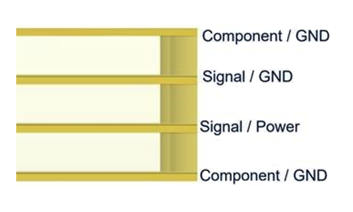 Figure 4. (Source: Antenova Ltd)
Tuning the Antenna for Performance
If the ground plane cannot reach the ideal length, consider these alternatives:
- Region‑specific tuning. Narrow the antenna’s operational band to match a specific country’s 4G allocation, improving efficiency.
- Active tuning networks. Add a PI matching network near the feed point to compensate for bandwidth loss on small ground planes (< 75 mm). RF specialists often help design these circuits.
Figure 5 displays a matching network on an evaluation board.
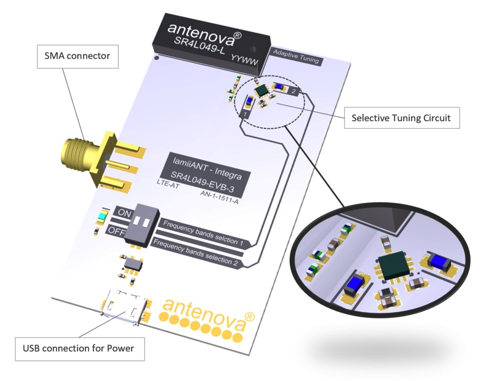 Figure 5. (Source: Antenova Ltd)
Designing the Transmission Line
Once the PCB material, thickness, and dielectric constant are defined, a co‑planar transmission line can be designed using standard RF trace tools. This ensures a 50 Ω characteristic impedance that matches the transceiver and power amplifier.
Antenova offers a free RF transmission‑line calculator to aid designers.
Additional Considerations
When multiple antennas share a PCB, spatial separation and orthogonal orientation are essential to maintain isolation. For MIMO systems, careful layout keeps cross‑correlation low.
Figure 6 shows proximity configurations for diversity.
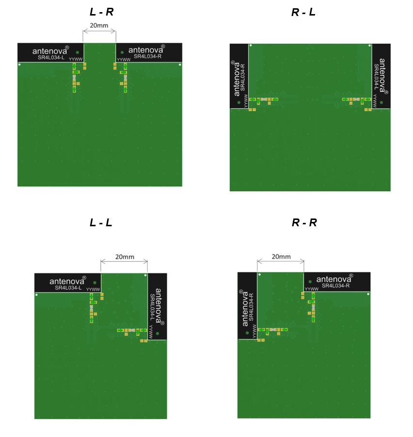 Figure 6. (Source: Antenova Ltd)
Figure 7 illustrates opposed configurations for diversity.
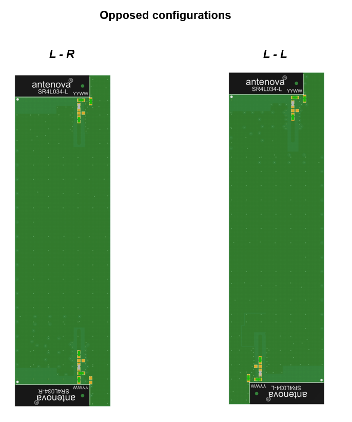 Figure 7. (Source: Antenova Ltd)
Enclosures should avoid metallic parts near the antenna; even metalised coatings can shift resonance and reduce bandwidth. Metallic proximity can also block radiation and degrade the overall pattern.
Conclusion
When incorporating an antenna into a small‑PCB design, begin by selecting the antenna and placing it first. This “antenna‑first” approach ensures that RF performance is optimised before other components are added, greatly increasing the likelihood of successful carrier approval. While regulatory bodies impose strict efficiency requirements, AT&T has relaxed thresholds for devices smaller than 107 mm.
Adopting these guidelines helps designers create compact, efficient, and compliant wireless products.
Embedded
- Getting Started with Python: Install, Run, and Write Your First Program
- 5 Key Wireless Standards Powering IoT Connectivity
- Xilinx Launches Zynq RFSoC DFE – A High‑Performance, Power‑Efficient Hard IP Solution for 5G Radios
- Maxim’s MAX86150: Integrated PPG & ECG Module for Mobile Health Monitoring
- Preparing Your Manufacturing Business for Industry 4.0: A Practical Roadmap
- Why Small Manufacturers Should Export: Key Benefits & a Practical Starter Guide
- Wireless Power Revolutionizing Modern Manufacturing: Efficiency, Safety, and Growth
- Begin Your Industry 4.0 Journey: A Practical Guide
- HP Executive Ramon Pastor Explains How Edge Computing & AI Enhance 3D Printer Security & Performance
- Beginner’s Guide: Setting Up RoboDK on Raspberry Pi