


Crystalline‑Si Solar Cells with a Black‑Silicon Rear Layer: Enhanced Efficiency Through Graded Band‑Gap Engineering
Abstract
We investigated crystalline‑silicon (c‑Si) solar cells that incorporate a black‑silicon (b‑Si) layer at the rear surface. Chemical etching produced the nanostructured b‑Si, and its presence at the back of the device led to a remarkable 27.7 % relative increase in power‑conversion efficiency compared with an equivalent cell lacking the b‑Si layer. The improvement is attributed to a graded band‑gap that forms at the rear, driving free electrons away from the high‑surface‑area b‑Si and thereby suppressing surface recombination. This study demonstrates that a rear‑side b‑Si layer can be leveraged to extend the spectral response of c‑Si solar cells into the sub‑band‑gap near‑infrared region.
Background
Highly textured silicon that has been loaded or doped with metal or non‑metal ions exhibits broadband absorptivity, giving rise to the so‑called black‑silicon (b‑Si) effect.1–6 Such Si has attracted attention for broadband photovoltaic applications.7–9 Existing work typically places the b‑Si layer at the front of the cell,10–19 which prevents sub‑band‑gap near‑infrared (NIR) photons from generating usable charge carriers because the generated electron‑hole pairs are too far from the PN junction. We hypothesised that positioning the b‑Si layer at the rear would allow the built‑in field at the Si/oxide interface, or an interdigitated back contact field, to separate NIR‑generated carriers and enable sub‑band‑gap photovoltage. However, the large specific surface area of b‑Si could introduce severe surface recombination.10,15,22 This work explores the photovoltaic response of c‑Si cells with a rear‑side b‑Si layer and elucidates the underlying physics.
Methods
Materials
We used a p‑type Si<100> wafer (CZ, double‑side polished, 10 × 10 × 0.2 mm³, 1–10 Ω·cm). The wafer was ultrasonically cleaned, dipped in 1 % HF, and then etched in a NaOH/alcohol/H₂O (0.5 g / 200 mL / 200 mL) solution at 90 °C for 15 min to create a slight antireflection texture. For rear‑side b‑Si formation, a 3 nm Ag catalyst layer was evaporated onto one surface. The wafer was then immersed in a 1 : 5 : 10 HF(40 %) : H₂O₂(30 %) : H₂O solution for 120 s at room temperature, yielding the nanostructured b‑Si. A phosphorous paste was deposited on the opposite surface, followed by 900 °C/20 min annealing in nitrogen to form the PN junction. Surface passivation was achieved with 20‑nm SiO₂ on the front and 10‑nm Al₂O₃ on the rear (the latter by ALD). An 80‑nm ITO front electrode and a 2‑µm Al rear electrode were deposited, and the cell was finally annealed at 425 °C/5 min in nitrogen.
Measurements
Reflectance spectra were recorded with a Shimadzu UV‑3101PC spectrophotometer. Surface morphology was examined by a Philips XL 30 SEM. Photovoltaic parameters were measured using an Oriel/Newport 94023A solar simulator under AM 1.5G 1 Sun. External quantum efficiency (EQE) was obtained on an Oriel/Newport QE system. Transmission electron microscopy (TEM) employed a JEOL EM‑3000. Photoluminescence (PL) used an Ocean Optics USB2000 with a 325‑nm He‑Cd laser. Contact potential difference (CPD) measurements were performed with a KP Technology SKP5050 Kelvin probe.
Results and Discussion
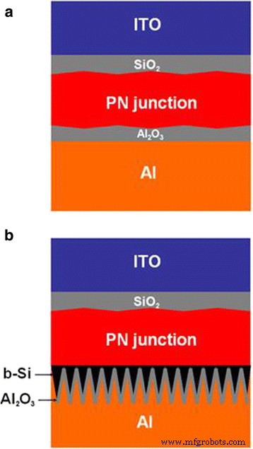
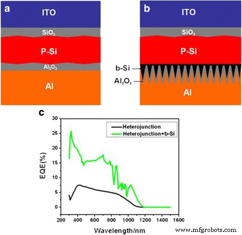
Figure 1 shows schematic cross‑sections of a slightly textured c‑Si cell with and without rear‑side b‑Si. The cell thickness is ≈ 200 µm.
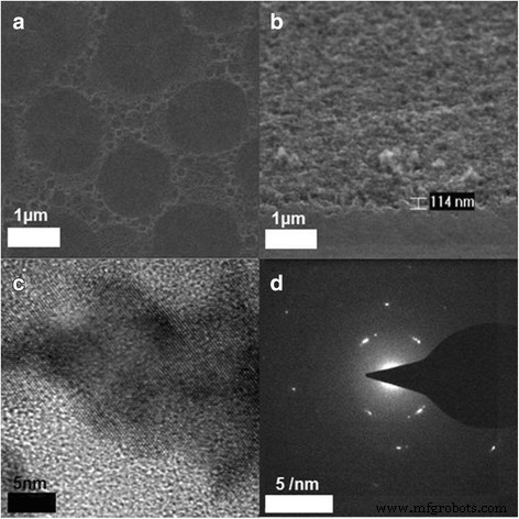
SEM images (Figure 2) reveal that the front surface has nanostructures of 10–20 nm, while the rear b‑Si exhibits an average height of ≈ 110 nm. HRTEM confirms nanocrystalline Si in the b‑Si, supported by the SAED pattern.
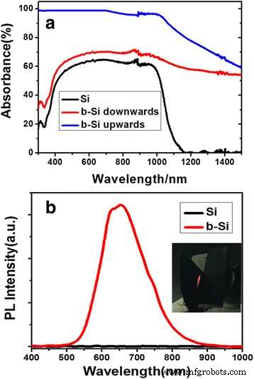
Absorption spectra (Figure 3a) demonstrate that b‑Si facing the incident light significantly enhances absorption across 300–1100 nm and introduces sub‑band‑gap NIR absorption, attributable to impurity‑level formation within the bandgap. When b‑Si faces away from the light (b‑Si downwards), absorption remains high in the 300–1100 nm range, indicating that the rear‑side b‑Si can still capture NIR photons.
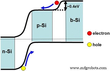
Four device variants were fabricated: (1) wafer Si; (2) wafer Si + Al₂O₃ rear passivation; (3) b‑Si rear; (4) b‑Si rear + Al₂O₃. Current‑voltage and EQE data (Figure 4) reveal that the wafer + Al₂O₃ device outperforms the unpassivated wafer, confirming effective surface‑recombination suppression. Surprisingly, the b‑Si rear device shows a 27.7 % relative efficiency increase over the plain wafer, despite the large surface area that would normally raise recombination. Adding Al₂O₃ to the b‑Si rear further boosts performance, underscoring that the rear passivation remains effective. The key to this improvement is a graded band‑gap at the rear: the b‑Si’s conduction band minimum lies ≈ 0.4 eV above that of p‑type Si (CPD measurement), creating a barrier that drives electrons away from the high‑surface‑area b‑Si while allowing holes to reach the rear electrode, thereby suppressing recombination.
Additional heterojunction PV devices (Figure 6) confirm the beneficial role of rear‑side b‑Si. The EQE of the b‑Si device is markedly higher than that of the device without b‑Si, consistent with the graded‑band‑gap mechanism.
Conclusions
Incorporating a black‑silicon layer at the rear of a crystalline‑silicon solar cell dramatically improves device performance by forming a graded band‑gap that mitigates surface recombination. The resulting efficiency gain of 27.7 % demonstrates the viability of rear‑side b‑Si for extending the spectral response of c‑Si cells into the sub‑band‑gap NIR region, paving the way for broadband photovoltaic technologies.
Nanomaterials
- High‑Efficiency (20.19 %) Inverted‑Pyramid Single‑Crystalline Silicon Solar Cell Fabricated via Optimized Metal‑Assisted Chemical Etching
- Optimizing Perovskite Solar Cell Efficiency with Size‑Controlled Ag Nanoparticles in a TiO₂ Compact Layer
- Optimizing Broadband Light Absorption in Thin‑Film Silicon Solar Cells with Double‑Sided Pyramid Gratings
- Enhanced Organic–Nanostructured Silicon Hybrid Solar Cells via Surface Modification for Superior Efficiency
- High-Performance Silicon Nanowire Heterojunction Solar Cells Using Al₂O₃ Passivation via Atomic Layer Deposition
- Boosting PERC Solar Cell Performance: ALD‑Deposited Al₂O₃ with Optimized Two‑Step Annealing for Superior Si Passivation
- Boosting PERC Cell Efficiency by Minimizing Interface Traps with High-Density Hydrogen Treatment
- Optimizing Niobium-Doped Titanium Oxide Layers for Enhanced Silicon Quantum Dot Solar Cells
- Speed-Locking of Particles on Graphene under Traveling Surface Waves
- KUKA flexibleCUBE: Modular Welding Cell for Advanced Automation