


Analog In‑Memory Computing: Power‑Efficient Edge AI Inference
Machine learning and deep learning are now woven into everyday technology. From natural‑language assistants to real‑time object detection, AI drives a growing number of consumer and industrial devices. Yet most of these applications rely on cloud‑based inference engines—an architecture that raises concerns about privacy, power consumption, latency and cost.
Deploying AI locally on the edge can eliminate those problems. The main hurdle is the memory‑driven power drain of conventional digital neural‑network accelerators. When weights and activations are fetched from DRAM or SRAM, the data movement alone consumes two to three orders of magnitude more energy than the arithmetic itself. Analog in‑memory computing tackles this bottleneck by performing multiply‑accumulate (MAC) operations directly inside a non‑volatile memory array.
Cloud‑Based AI: The Pain Points
When an edge device forwards raw data to a remote server, several issues arise:
- Privacy & security – Personal or confidential information is transmitted and stored in data centers.
- Unnecessary power use – Every bit sent over the radio, stored in the cloud and re‑retrieved burns energy.
- Latency for small‑batch inference – Responses can take more than 100 ms, which is perceptible to users.
- Data‑economy inefficiency – Sensors generate massive streams; uploading everything is neither economical nor sustainable.
To overcome these challenges, a trained model is first built on a high‑performance platform (cloud, GPU farm, etc.). The resulting weights are then mapped to a lightweight inference engine that performs the computation locally.
The MAC‑Heavy Nature of Neural Networks
Even lightweight models are dominated by MACs. For example, MobileNet‑v1 with a 224×224 input contains 4.2 million parameters and requires 569 million MACs per inference. The multiplication and accumulation are performed in a dense matrix‑vector product.
Why Digital Computing Struggles
In a conventional accelerator, weights and activations are stored in DRAM/SRAM and must be fetched into an arithmetic logic unit (ALU). Figure 3 illustrates the memory bottleneck: the energy spent moving data (50–100 pJ per transfer) dwarfs the 250 fJ per MAC operation. Even with aggressive data‑reuse techniques, the Von Neumann architecture imposes a hard limit on power efficiency.
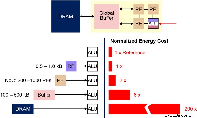 Figure 3: Memory Bottleneck in Machine Learning Computation. (Source: Y.-H. Chen, J. Emer, and V. Sze, “Eyeriss: A Spatial Architecture for Energy‑Efficient Dataflow for Convolutional Neural Networks,” ISCA, 2016.)
Analog In‑Memory Computing to the Rescue
By embedding computation into the memory array itself, the need to shuttle weights disappears. The remaining data transfer is limited to the input signal, which is typically a sensor output. Flash cells operating in the sub‑threshold regime consume sub‑nanoamp currents, making active power negligible. In standby, the non‑volatile cells retain data without any power draw.
The memBrain™ platform from Silicon Storage Technology (a Microchip company) exemplifies this approach. Built on the SuperFlash® (ESF3) memory technology, each bitcell can be programmed to a precise threshold voltage (Vt), establishing a conductance that represents a weight. When an input voltage is applied, the current through the cell equals the product of the input and the stored weight.
Multi‑Level Memory Architecture
Figure 4 shows the cross‑section of an ESF3 bitcell. The cell includes five terminals—Control Gate (CG), Word Line (WL), Erase Gate (EG), Source Line (SL), and Bitline (BL). High‑voltage EG programs the floating gate, while low‑voltage biasing on the other terminals reads or writes the cell.
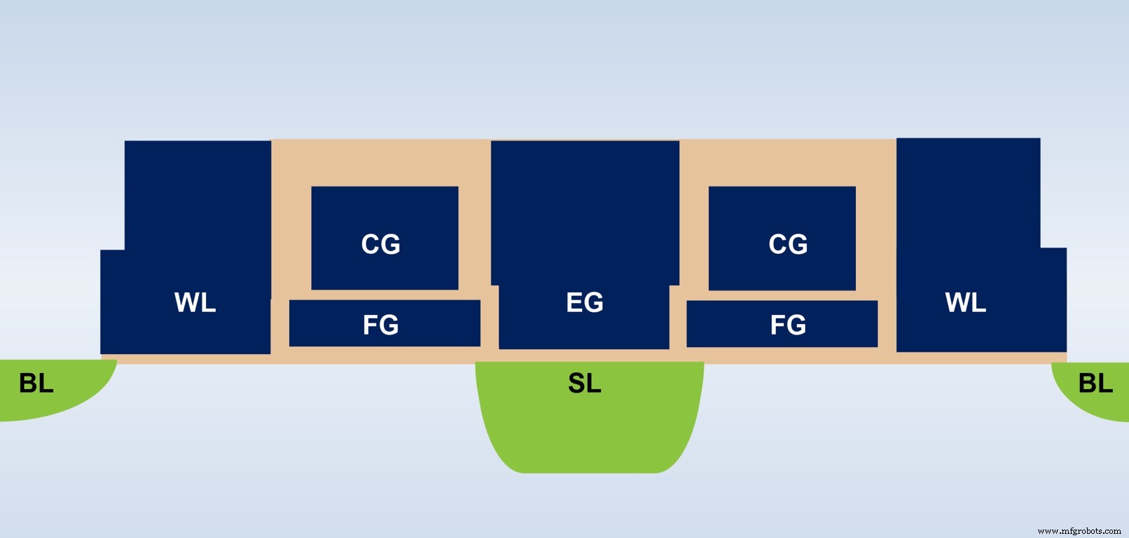 Figure 4: SuperFlash ESF3 Cell. (Source: Microchip Technology)
Fine‑grained programming tunes the floating‑gate Vt to produce a specific I‑V curve. Figure 5 demonstrates a 2‑bit example where four distinct Vt levels yield four separate current responses when a fixed CG voltage is applied.
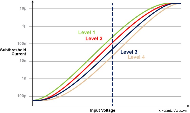 Figure 5: Programming Vt Levels in ESF3 Cell. (Source: Microchip Technology)
MAC in the Memory Array
Each cell’s conductance gm embodies a trained weight. The current Iout = gm · Vin implements the multiply step. By wiring many cells in parallel, the column currents naturally sum, yielding the accumulate operation. Figure 6 visualises a 2×2 array performing two MACs and one accumulation.
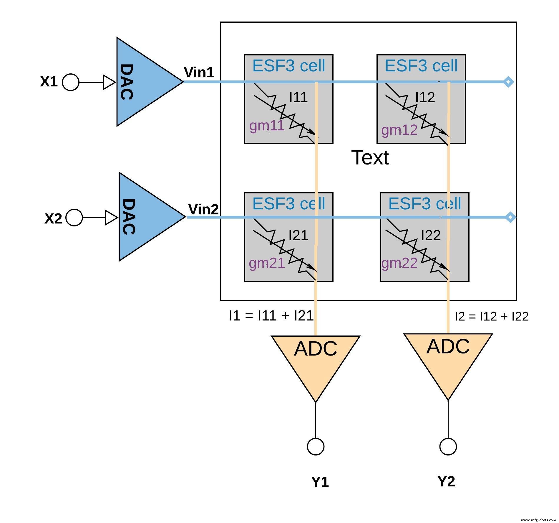 Figure 6: Multiply‑Accumulate Operation with ESF3 Array (2×2). (Source: Microchip Technology)
On a larger scale, a weight matrix can be mapped onto a single memory array. Figure 7 shows the matrix layout for a fully connected layer.
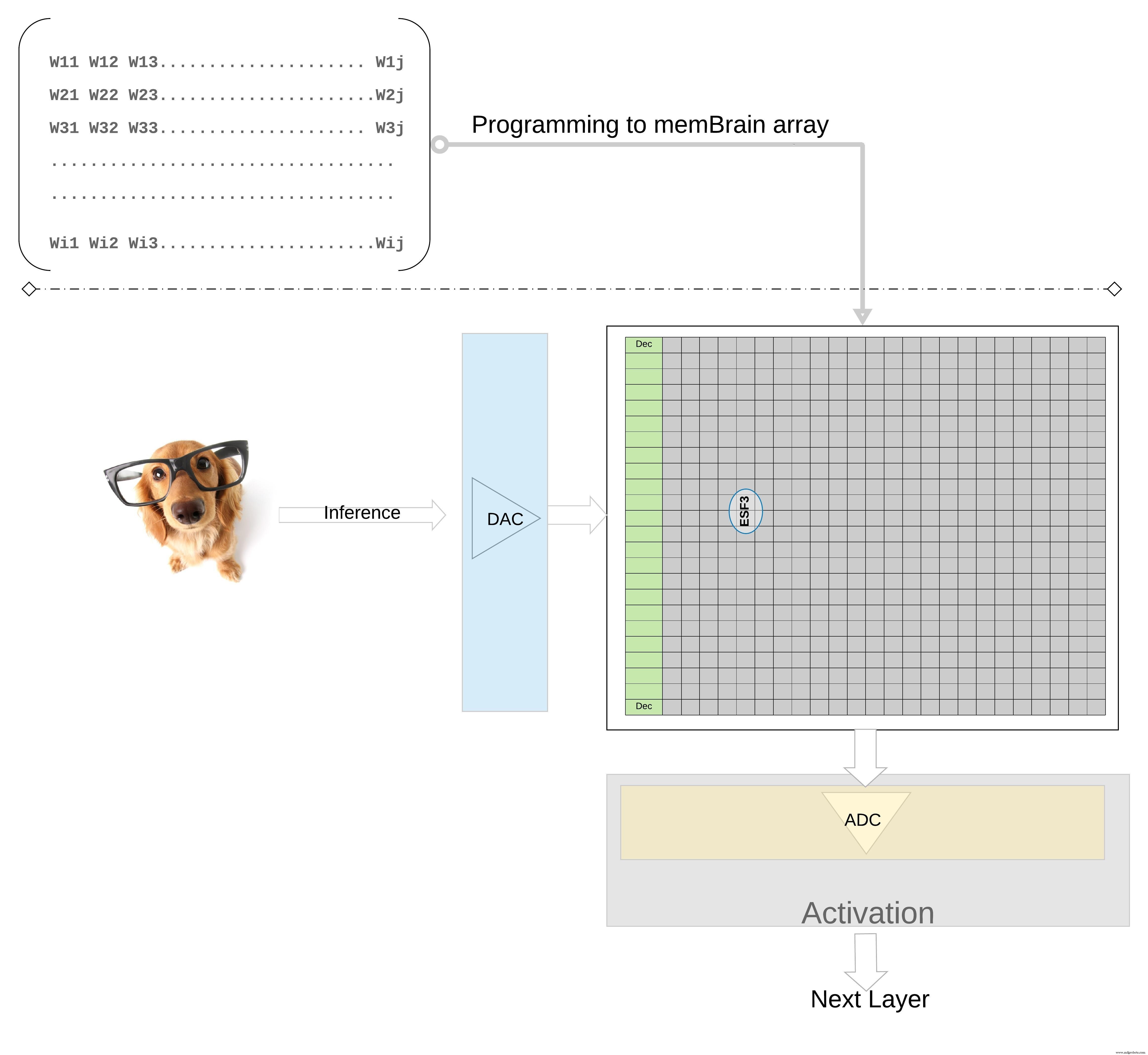 Figure 7: Weight Matrix Memory Array for Inference. (Source: Microchip Technology)
The inference flow is straightforward: sensor data is digitised, converted to an analog voltage by a DAC, fed into the array, and the resulting column currents are digitised by an ADC for subsequent activation and pooling stages.
Modularity and Scalability
memBrain tiles are designed to be stacked. Figure 8 shows a 3×4 configuration where multiple tiles share a common analog‑digital interconnect. Data moves across tiles via a shared bus, enabling the construction of deep networks without a single monolithic die.
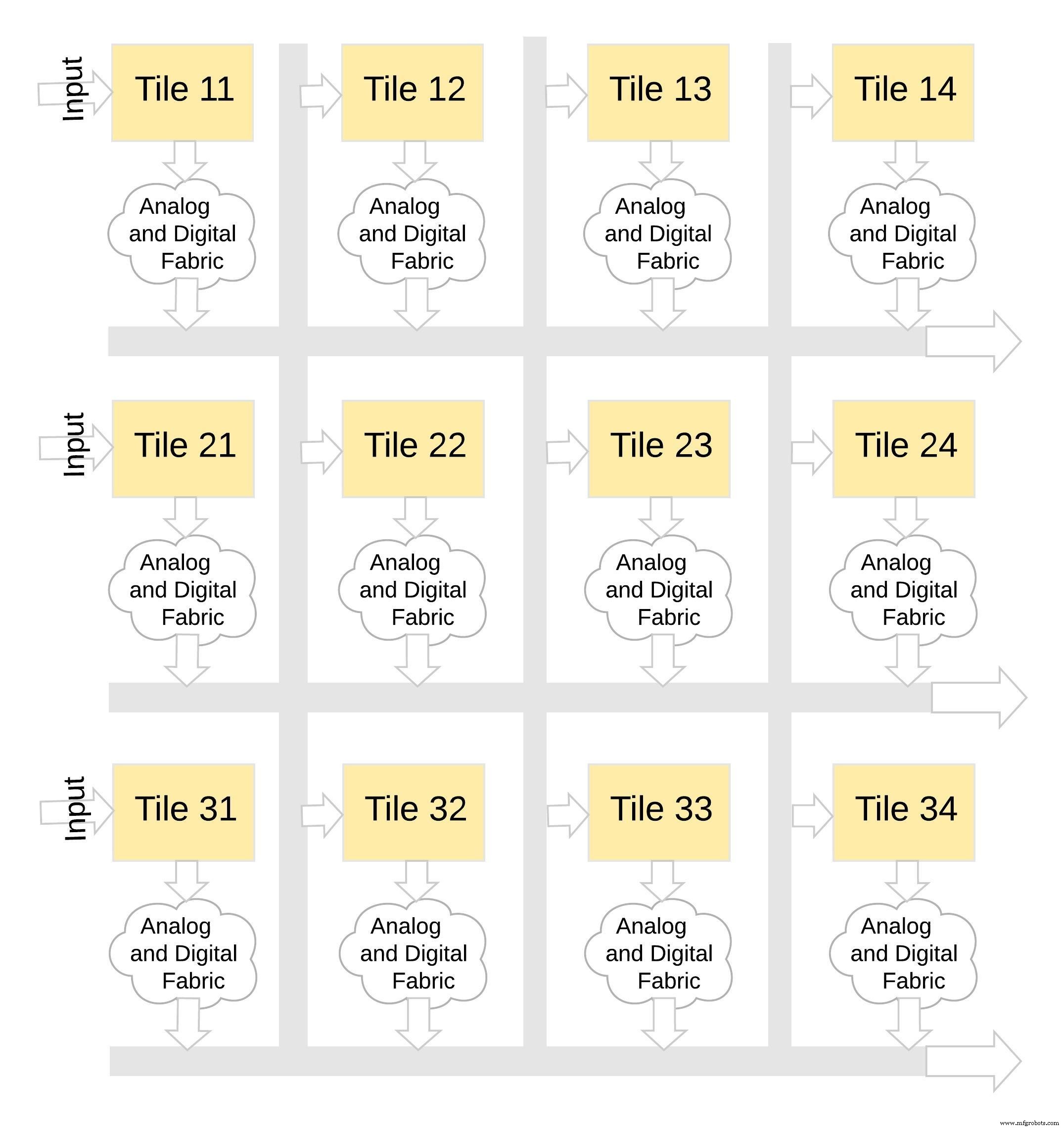 Figure 8: memBrain™ is Modular. (Source: Microchip Technology)
Software Development Kit (SDK)
The accompanying SDK is framework‑agnostic. Whether you train in TensorFlow, PyTorch, or another library, the SDK handles model quantisation, mapping, and deployment to the memBrain hardware. Figure 9 outlines the workflow from training to inference.
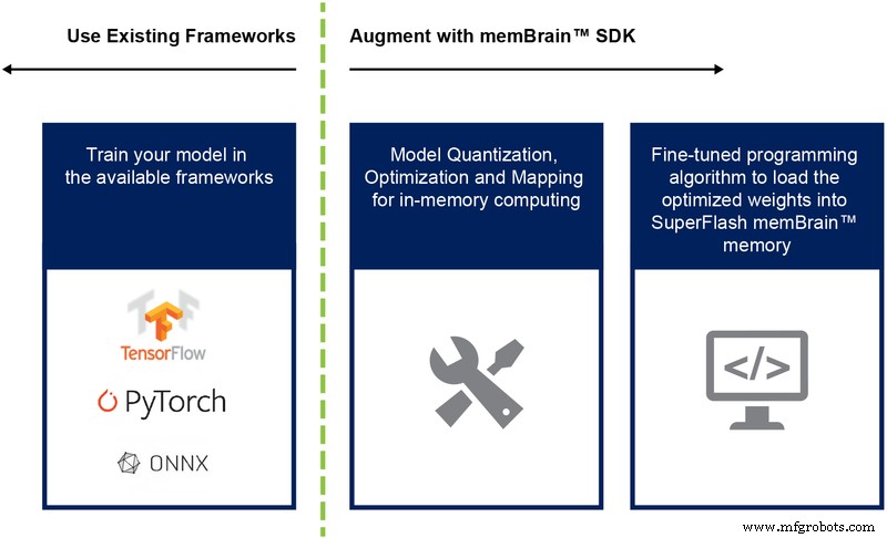 Figure 9: memBrain™ SDK Flow. (Source: Microchip Technology)
Key Advantages
- Ultra‑low power – In‑memory compute eliminates data movement, flash cells operate sub‑threshold, and no standby power is needed. The architecture also exploits sparsity, as zero weights or inputs leave cells idle.
- Compact footprint – The 1.5‑transistor split‑gate cell stores a 4‑bit value, whereas a 6‑transistor SRAM would require 24 transistors for the same data. The result is a dramatically smaller die area.
- Reduced development cost – By leveraging mature flash processes and avoiding the need for ultra‑dense geometries, mask set costs and lead times are significantly lowered compared to ASICs designed for edge AI.
Edge AI promises transformative applications, but power and cost remain limiting factors. Analog in‑memory computing, backed by proven multi‑level flash technology, offers a practical, low‑cost pathway to bring intelligent inference right to the sensor.
Embedded
- Industrial Edge Computing: How It Drives Manufacturing Performance
- How Automotive OEMs Overcome Additive Manufacturing Challenges with Digital Solutions
- IoT Edge Computing: Bridging Devices and Cloud for Real‑Time Insights
- Mastering Low‑Power Modes on Arm Cortex‑M: Practical Tips & Energy Savings
- Edge Computing: 5 Potential Pitfalls—and How to Overcome Them
- Leveraging IIoT Data to Drive Profitability in Lean Manufacturing
- Edge Computing: The Catalyst Driving Industry 4.0 Forward
- Leveraging Connected Technology to Resolve Key Supply Chain Challenges
- Harnessing IoT Edge Computing for Real‑Time Data Analysis
- Overcoming Edge Computing Challenges: Proven Strategies for Real-Time Data Processing