


Exploring Voltera: A Journey into Canadian PCB Printing Innovation
Years ago, our colleague Max published a compelling blog titled Want a Voltera Desktop PCB Printer?, detailing a groundbreaking PCB printer being developed in Canada and funded through Kickstarter. The concept was intriguing, but the fact that it was a Canadian endeavor sparked my curiosity. After signing up for the mailing list, a postcard announcing the finished product arrived, and I shared it with my supervisor. He immediately requested a demonstration. When we inquired, Voltera invited us to visit their facility in Kitchener—a one‑hour road trip away.
In recent months, Canada has seen a notable surge in tech innovation. Many attribute this uptick to the ripple effect of BlackBerry’s decline, which prompted engineers to pivot toward entrepreneurial ventures. BlackBerry’s headquarters are in Waterloo, Ontario—a city that is part of a larger metropolitan area comprising Kitchener, Waterloo, and Cambridge. Interestingly, Kitchener was originally named Berlin by German immigrants but was renamed in 1916 to honor the British Secretary of State for War. This historical tidbit reminds us that Voltera is located in Kitchener.

Lord Kitchener in a well‑known pose. (Source: Wikipedia)
The University of Waterloo is renowned for its engineering and scientific programs, boasting one of Canada’s most prominent co‑op engineering curricula. To nurture innovation, the university operates the Velocity Garage, the world’s largest free startup incubator. Voltera occupies a space within this incubator.
The building resembles a converted warehouse turned student union: communal meeting rooms, shared kitchen facilities, and individual startup areas with minimal partitioning. Adjacent to Voltera’s workspace is a dedicated workshop equipped with secure doors, reflecting the company's focus on intellectual property protection. Visiting this environment gave me insight into the collaborative ethos I discussed in my post How Well Can You Work With Others? and highlighted the significance of tools like Upverter in Canada’s innovation ecosystem.
For those interested in seeing Voltera in action, the company’s website hosts numerous videos and images, and additional footage is available on YouTube.
Mechanically, the V‑One resembles a sophisticated X‑Y plotter. It features an X‑Y controlled carriage with an adjustable Z axis, and a thermally controlled print bed. The carriage supports interchangeable heads—an important design choice that balances versatility with cost. These heads include a conductive‑ink cartridge with a nozzle, a solder‑paste cartridge, and a probe for surface mapping.
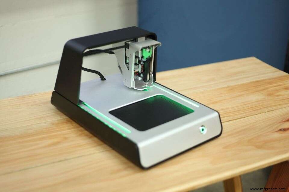
Figure 2: The V‑One. The heating pad is the flat black rectangular area and the carriage with a conductive‑ink cartridge is visible at the top right. (Source: Voltera)
The V‑One targets the high‑end hobbyist and entry‑level professional market, which explains some manual operations—such as head changes—to keep costs reasonable. Despite these manual steps, the device achieves impressive placement accuracy.
Before printing, users must provide a Gerber‑formatted PCB design. The workflow begins by clamping the blank PCB onto the heated bed, inserting the probe into the carriage, and performing X‑Y calibration. For trace deposition, the nozzle must hover within tight tolerances above the PCB. The probe maps surface undulations, creating a 3‑D profile that guides precise ink placement. On blank PCBs the exact alignment is less critical, but for finished boards fiducials are aligned manually to the probe’s reference points.
Trace deposition uses an ink‑jet–style process: conductive ink is atomized and accelerated with high voltage. The ink is extruded under pressure generated by a gear‑driven mechanism atop the cartridge. Deposition is swift, typically completing a complex side in a matter of minutes. A flow‑rate adjustment allows fine‑tuning to match specific board requirements. Once deposited, the traces remain wet and must be handled carefully; they are then cured on the heated bed, a process that takes roughly 30 minutes.
Embedded
- Amber: From Ancient Resin to Scientific Treasure – History, Properties, and Modern Uses
- The Guillotine: History, Design, and Legacy
- Silicon: Properties, Production, and Market Outlook
- The Ukulele: From Portuguese Roots to Modern Craftsmanship
- The Complete Guide to the U.S. Chicken Industry: History, Production, and Quality Control
- Compost: The Ultimate Soil Enrichment Solution
- Gelatin: From Ancient Protein to Modern Applications – Production, Uses, and Safety
- The Evolution and Manufacturing of Modern Pin‑Tumbler Locks
- Vodka: From Ancient Distillation to Modern Production
- Macadam Explained: The Historic Road Construction Technique