


High-Performance Perovskite Transistors Now Printable: POSTECH Breakthrough
A Pohang University of Science and Technology (POSTECH) research team has improved the performance of a p-type semiconductor transistor using inorganic metal halide perovskite. One of the biggest advantages of the new technology is that it enables solution-processed perovskite transistors to be simply printed as semiconductor-like circuits.
Perovskite-based transistors control the current by combining p-type semiconductors that exhibit hole mobilities with n-type semiconductors. Compared to the n-type semiconductors that have been actively studied so far, fabricating high-performance p-type semiconductors has been a challenge.
Many researchers have tried to utilize perovskite in p-type semiconductors for its excellent electrical conductivity, but its poor electrical performance and reproducibility have hindered commercialization.
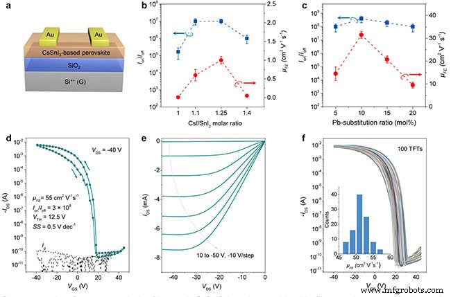
To overcome this issue, the researchers used the modified inorganic metal halide: caesium tin triiodide (CsSnI3), to develop the p-type perovskite semiconductor and fabricated the high-performance transistor based on this. The transistor exhibits high hole mobility of 50cm2V-1s-1 and more and an on/off current ratio of more than 108. This is the highest recorded performance among the perovskite semiconductor transistors that have been developed so far.
By making the material into a solution, the researchers succeeded in simply printing the p-type semiconductor transistor as if printing a document. Since this method is not only convenient but also cost-effective, it can lead to the commercialization of perovskite devices in the future.
“The newly developed semiconductor material and transistor can be widely applicable for logic circuits in high-end displays and in wearable electronic devices. They can also be used in stacked electronic circuits and optoelectronic devices by stacking them vertically with silicon semiconductors,” explained Professor Yong-Young Noh.
Sensor
- Choosing Between 3D Printing and Machining for Prototypes: When Each Method Wins
- 3DP – Accelerating Packaging with 3D‑Printed Tools: Boost Design, Cut Costs, and Scale Rapidly
- Solution‑Processed Nanocrystalline CuAlO₂ Thin‑Film Transistors: Optimized p‑Type Performance for Low‑Cost CMOS Applications
- High‑Performance Perovskite Photodetector via Trilayer EA/TiO₂ Architecture
- Enhanced Performance of CsPbI₂Br Perovskite Solar Cells via ZnCl₂–MnCl₂ Doping
- Enhanced Quasi‑2D Perovskite LEDs with Poly(vinylpyrrolidone) Treatment: Record Brightness & Efficiency
- Custom 3D‑Printed Stepper Motor: Build Your Own Precision Drive
- Enhancing Parts with 3D Printed Lattice Structures
- Transforming Prototyping: The Power of 3D‑Printed Tooling
- Revolutionizing Sustainability: Fully Recyclable Printed Electronics