


In Situ Formation of CdS and Sb₂S₃ Nanocrystals within P3HT:PC₆₁BM Enhances Photocurrent in Inverted Hybrid Solar Cells
Abstract
Incorporating nano‑heterostructures into the active layer of bulk heterojunction solar cells can markedly improve device performance. Here we report the in‑situ generation of CdS or Sb₂S₃ nanocrystals within a P3HT:PC₆₁BM blend by adding cadmium or antimony xanthate precursors to the polymer solution. Upon thermal annealing, the precursors decompose to form uniformly dispersed nanocrystals, creating an intimate polymer–nanocrystal interface that enhances optical absorption, hole mobility, and surface roughness. Devices fabricated with 3 wt % CdS or Sb₂S₃ exhibit power‑conversion efficiencies (PCEs) of 2.91 % and 2.92 % respectively—substantially higher than conventional P3HT:PC₆₁BM cells. UV–Vis, SCLC, and AFM studies confirm the improved charge transport and morphological benefits conferred by the nanocrystals, underscoring the effectiveness of in‑situ synthesis for high‑efficiency hybrid solar cells.
Background
Organic photovoltaic (OPV) technologies offer light‑weight, low‑cost, and flexible solutions, while inorganic semiconductors provide high charge mobility and chemical stability. Hybrid solar cells (HSCs) that combine these two material classes aim to harness the best of both worlds. Traditional approaches blend pre‑synthesized, ligand‑capped inorganic nanocrystals with the polymer matrix, but long‑chain ligands create insulating barriers and the use of cosolvents can disturb polymer chain ordering, limiting charge transport and efficiency. In contrast, in‑situ synthesis of inorganic nanoparticles directly within the polymer film eliminates surfactants and cosolvents, promoting intimate mixing and efficient photo‑induced charge transport.
Previous studies have shown that metal‑sulfide nanocrystals such as CdS and Sb₂S₃ can serve as electron cascades or dopants, improving charge extraction and light absorption in P3HT:PC₆₁BM blends. However, achieving optimal nanocrystal loading without compromising the polymer morphology remains a challenge.
Methods / Experimental
Device Fabrication
Inverted HSCs were assembled on patterned ITO/glass (10–15 Ω □⁻¹). A 10 nm CdS interface layer was spin‑coated from a 100 mg mL⁻¹ chlorobenzene solution of cadmium xanthate and annealed at 160 °C for 15 min under N₂. The active layer was prepared by blending 1:1 P3HT:PC₆₁BM (17 mg mL⁻¹) with 3 wt % (or 0, 5, 7 wt %) of the appropriate xanthate precursor. The film was spin‑coated at 600 rpm, then annealed at 160 °C for 30 min to decompose the precursor into CdS or Sb₂S₃ nanocrystals. An 8‑nm MoO₃ hole‑transport layer and a 100‑nm Ag anode were thermally evaporated through a shadow mask to define a 0.10 cm² active area.
Characterization
XRD (Cu Kα, 40 kV) assessed crystallinity, while TGA (10 °C min⁻¹, N₂) confirmed precursor decomposition. UV–Vis absorption was recorded with a U‑3900H spectrophotometer. Photovoltaic performance (J–V under 1 sun, AM 1.5G) was measured with a Keithley 2410 source meter in N₂. EQE/IPCE spectra were obtained using a calibrated silicon detector. Hole mobilities were extracted from SCLC measurements on hole‑only devices (ITO/PEDOT:PSS/active layer/MoO₃/Ag). AFM (tapping mode) provided surface morphology and roughness data.
Results and Discussion
Thermal Stability of Precursors
TGA revealed that cadmium xanthate decomposes between 50–150 °C, leaving ~25 % residue matching CdS (28 %), while antimony xanthate decomposes between 120–160 °C, yielding ~35 % residue consistent with Sb₂S₃ (35 %). These profiles guided the annealing conditions to ensure complete precursor conversion.
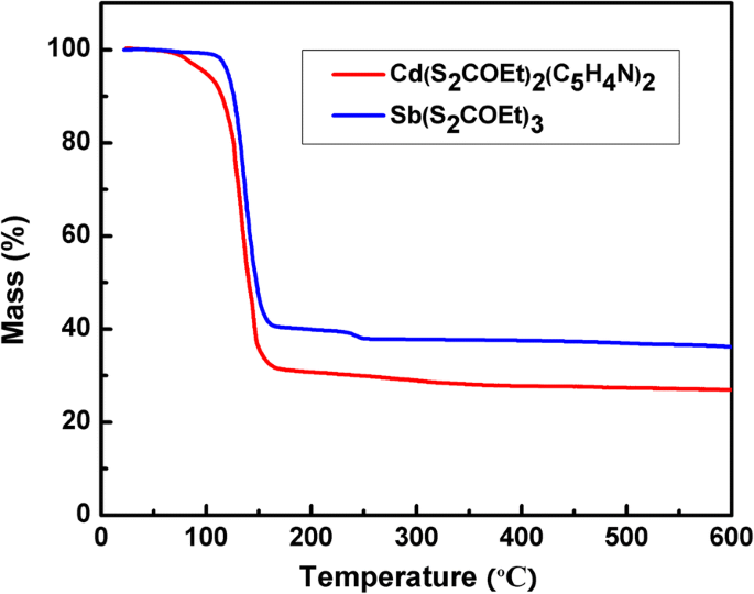
TGA plots of cadmium and antimony xanthates
Nanocrystal Formation and Morphology
Post‑annealing, the active layer displayed yellow or orange coloration indicative of CdS or Sb₂S₃ formation. XRD patterns confirmed hexagonal/cubic CdS and orthorhombic Sb₂S₃ phases, aligning with the TGA data. AFM showed increased surface roughness from 2.82 nm (pristine) to 8.89 nm (3 wt % CdS) and 7.13 nm (3 wt % Sb₂S₃), suggesting nanocrystal‑induced morphological changes that enhance interpenetration and exciton dissociation.
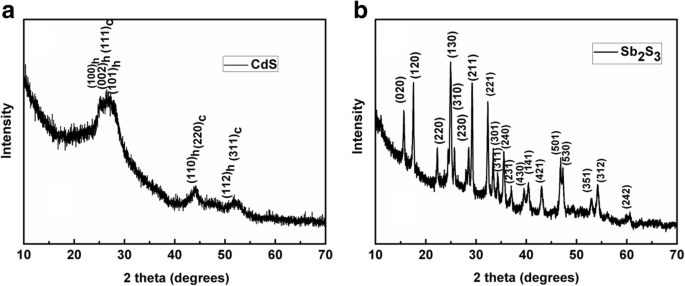
XRD patterns of CdS and Sb₂S₃ films
Photovoltaic Performance
J–V curves (Fig. 3b‑c) show that adding 3 wt % CdS or Sb₂S₃ raises the short‑circuit current (Jsc) from 7.77 mA cm⁻² to 8.72 mA cm⁻² (CdS) or 9.15 mA cm⁻² (Sb₂S₃). The series resistance drops from 22.15 Ω cm² to 16.70 Ω cm² (CdS) or 17.50 Ω cm² (Sb₂S₃), improving the fill factor from 0.52 to 0.56 or 0.54. The resulting PCEs peak at 2.91 % (CdS) and 2.92 % (Sb₂S₃), outperforming the control (2.34 %) and surpassing previously reported CdS‑doped P3HT:PC₆₁BM cells.
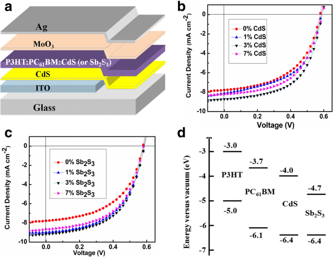
Fig. 3. a Device schematic. b J–V curves for CdS loading. c J–V curves for Sb₂S₃ loading. d Energy band diagram.
Spectral Response and Absorption
IPCE spectra (Fig. 4a) demonstrate higher quantum efficiencies across 300–650 nm for the nanocrystal‑doped devices. At 540 nm, the IPCE peaks reach 60 % (CdS) and 65 % (Sb₂S₃) versus 55 % for the pristine blend. UV–Vis absorption (Fig. 4b) shows modest enhancement for CdS and notable increase for Sb₂S₃, correlating with the improved Jsc.
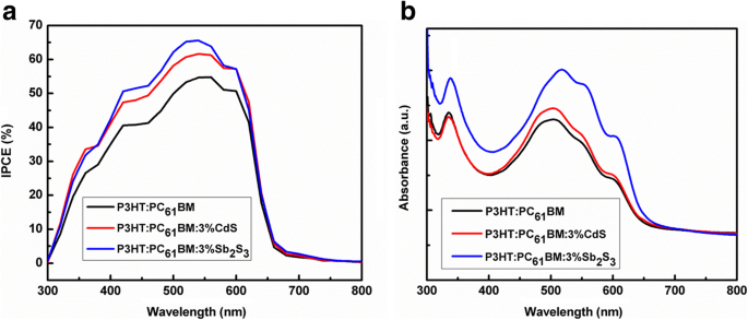
Fig. 4. a IPCE curves. b UV–Vis absorption spectra.
Charge Transport
SCLC measurements (Fig. 5) reveal that the hole mobility increases from 4.09 × 10⁻⁵ cm² V⁻¹ s⁻¹ (pristine) to 1.53 × 10⁻⁴ cm² V⁻¹ s⁻¹ (CdS) and 1.69 × 10⁻⁴ cm² V⁻¹ s⁻¹ (Sb₂S₃). The enhanced hole transport balances the inherently higher electron mobility of P3HT:PC₆₁BM, reducing recombination and boosting Jsc and FF.
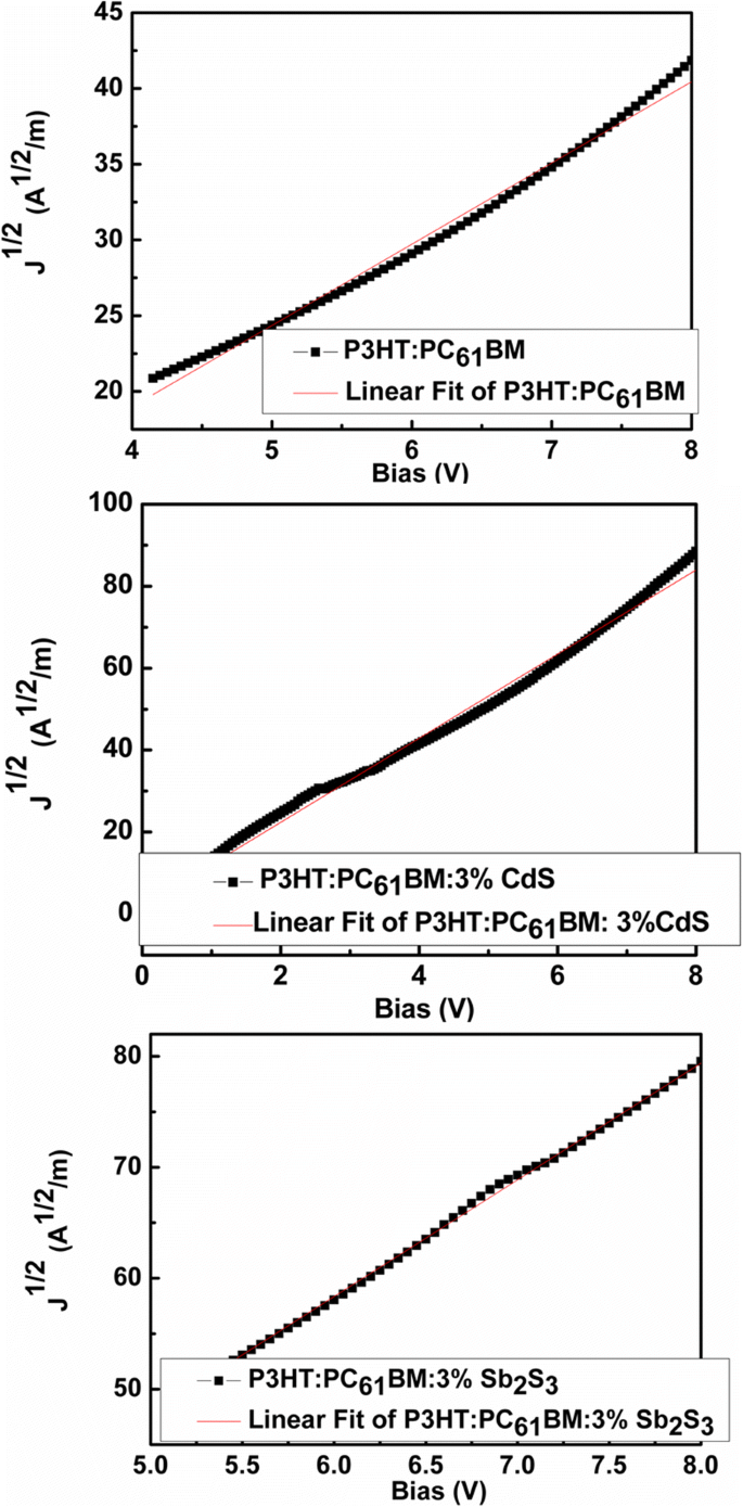
Fig. 5. J½–V curves for hole‑only devices.
Surface Morphology
AFM images (Fig. 6) confirm that the 3 wt % nanocrystal layers exhibit higher roughness, facilitating better contact with the MoO₃ hole‑transport layer and improving charge extraction. The increased interfacial area contributes to the observed gains in Jsc and FF.
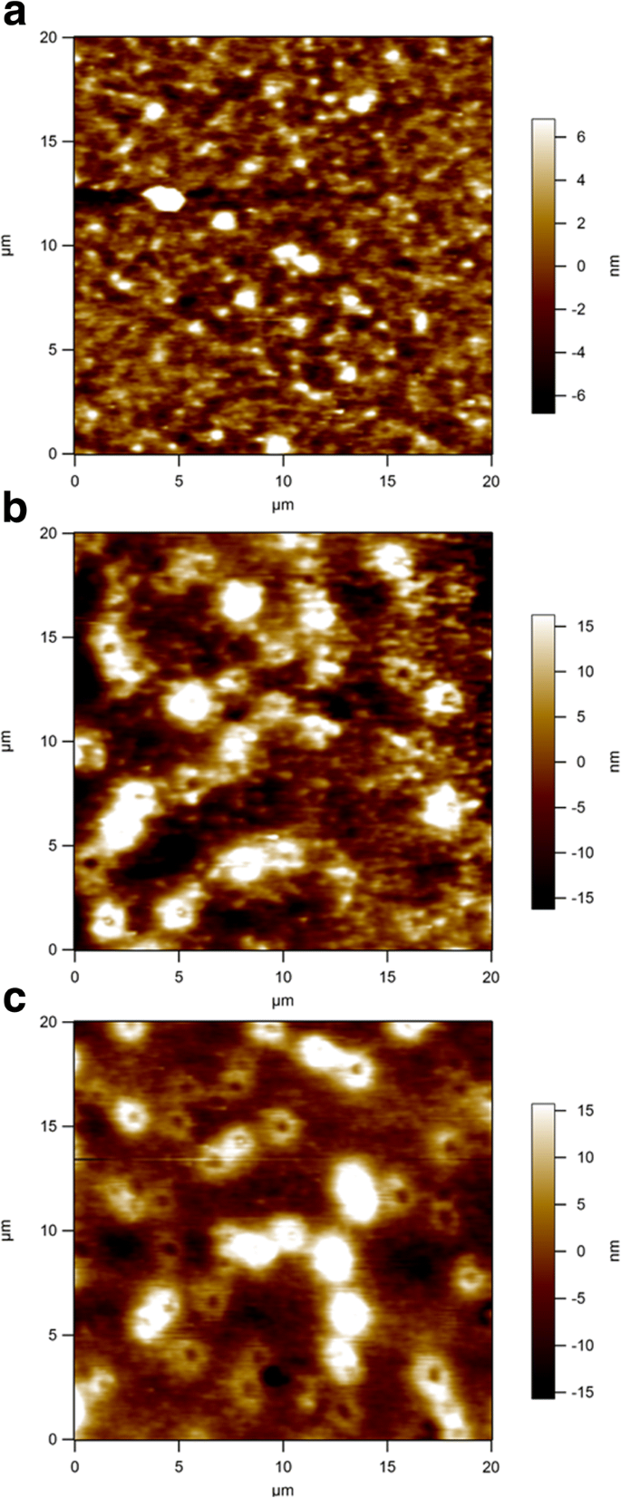
Fig. 6. AFM height images: a pristine, b 3 wt % CdS, c 3 wt % Sb₂S₃.
Conclusions
By in‑situ synthesizing CdS or Sb₂S₃ nanocrystals within a P3HT:PC₆₁BM matrix, we achieved 3 wt % doping that markedly enhances optical absorption, hole mobility, and surface roughness—key factors driving the highest reported PCEs of 2.91 % (CdS) and 2.92 % (Sb₂S₃) for inverted HSCs. This ligand‑free, solvent‑free approach offers a scalable pathway to high‑efficiency hybrid photovoltaics.
Nanomaterials
- Nano‑Heterojunctions: Boosting Solar Cell Efficiency with Colloidal Quantum Dots
- Methanol‑Enhanced PEDOT:PSS Hole Transport Layer Boosts Silicon/Organic Hybrid Solar Cell Efficiency to 12.2%
- GoldMag: PSS‑MA Coating Enhances Stability & Optical Precision for Protein Detection
- Controlled Hydrothermal Synthesis of ZnO Nanocrystals for Enhanced Inverted Polymer Solar Cells
- Superior Performance of Inverted Perovskite Solar Cells Using CdSe Quantum Dot and LiF Electron Transport Layers
- High‑Efficiency Planar Perovskite Solar Cells via Sequential Vapor‑Grown Hybrid Perovskite Layers
- Designing Plasmonic Nanoparticle Strategies for Enhanced Organic Solar Cell Performance
- Enhanced Photovoltaic Efficiency of GaAs Pin‑Junction Nanocone Solar Cells via Optimized Optical Absorption
- Thickness‑Dependent Photocurrent and Optoelectronic Dynamics in TiO₂/Sb₂S₃/P3HT Planar Hybrid Solar Cells
- Boosting Light Capture in Perovskite‑Silicon Tandem Solar Cells Using Nanohole Arrays