


IBM's Air Spacer Innovation Paves Way for 10 nm FinFET Chips
This is the third of a four‑part series on IBM’s cutting‑edge papers presented at IEDM 2016.
The International Electron Devices Meeting is widely regarded as the world’s premier forum for breakthrough research in semiconductor and electronic device technology, design, manufacturing, physics, and modeling. At this year’s conference in San Francisco, IBM showcased a scanning‑probe thermometer, an air‑spacer technique for 10 nm chips, a 7 nm device, and even carbon nanotube innovations—all aimed at extending Moore’s Law and exploring new architectures.
Among the four highlighted IBM papers, the third focuses on “Air Spacer for 10 nm FinFET CMOS and Beyond.” Dr. Kangguo Cheng, a senior technical staff member and Master Inventor at IBM Research’s Albany Nanotech Center, led the team that demonstrated how a simple air gap can dramatically lower parasitic capacitance in next‑generation transistors.
While 14 nm nodes are already manufacturable, the transition to 10 nm faces a critical obstacle: parasitic capacitance. As transistors shrink, the insulating gaps between contacts become proportionally smaller, allowing unwanted charge to accumulate. When a transistor switches, this stored charge is released, causing both slower signal propagation and higher power consumption—ultimately leading to increased heat and reduced reliability.
Dr. Cheng’s approach replaces these conductive gaps with air—an almost perfect insulator. By inserting an air spacer above the fin top, the team reduced transistor‑level capacitance by up to 25 % and achieved a 15 % reduction in a ring‑oscillator test circuit. The result is a 25 % power savings at the device level and a corresponding 15 % system‑wide improvement.
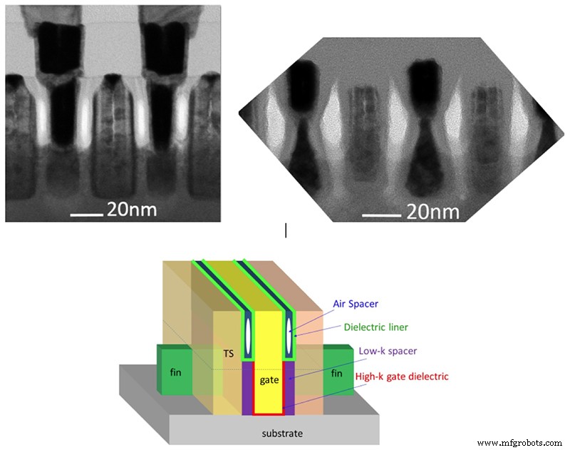
Top left: TEM image of a FinFET transistor with air spacers (the white spaces) at 10 nm dimensions. Top right: Damage after an aggressive spacer pulldown process; specifically, erosion of the fin and source/drain epitaxy. Bottom middle: Schematic of a partial air spacer structure. Air spacers are formed only above the fin top to minimize the impact on the gate stack. Dielectric liners protect gate stacks during air spacer fabrication.
By mitigating parasitic capacitance, air spacers enable more efficient 10 nm and 7 nm FinFET chips, and they hold promise for power‑saving 14 nm devices as well. IBM’s work illustrates how a material as simple as air can play a pivotal role in next‑generation semiconductor design.
Read part one: Mapping hot spots
Read part two: Another kind of chip with carbon nanotubes
Nanomaterials
- High‑Performance Tungsten‑Titanium Alloy Targets for Advanced Semiconductor Chips
- Ultra‑High‑Purity Tungsten Targets: Key to Advanced Semiconductor Thin Films
- IBM Scientist Unveils Carbon Nanotube Technology to Extend Moore’s Law
- Low‑Temperature ALD of In₂O₃ Nanofilms for High‑Performance Thin‑Film Transistors
- Optimized Air Blast System for Efficient Blast Furnace Operation
- Expert Guide to Maintaining Industrial Air Compressors
- Essential BGA Chip Layout Tips for Optimal Performance
- Choosing the Right Air Receiver Size: Optimize Performance & Efficiency
- Preventing Microbial Growth in Compressed Air Systems for Food & Beverage Processors
- Optimizing Snowmaking: The Role of Air Compressors in Quality Powder Production