


Ultra‑High‑Purity Tungsten Targets: Key to Advanced Semiconductor Thin Films

Ultra‑High‑Purity Tungsten Targets for Semiconductor Applications
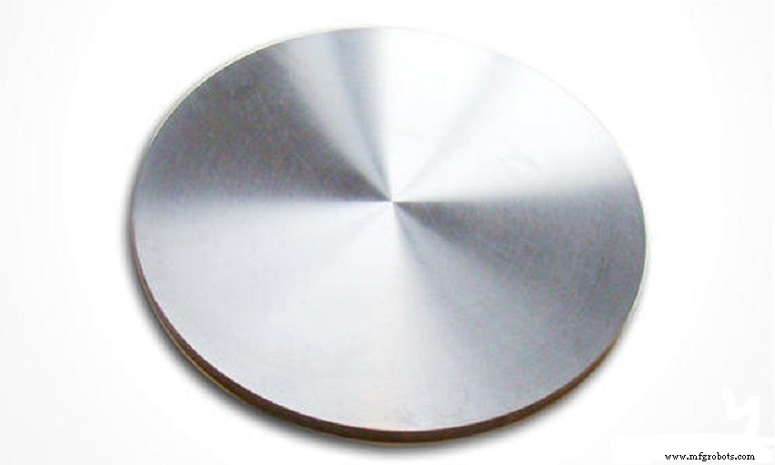
The tungsten target, engineered to exceed 99.95% purity, boasts a density of 19.35 g/cm³, minimal vapor pressure, and exceptional thermal stability. These attributes make it ideal for depositing ultra‑fine tungsten oxide films that serve as diffusion barriers, adhesive layers, and memory electrodes in contemporary semiconductor devices.
When integrated into chip manufacturing, tungsten oxide films enhance overall device performance by providing robust barrier properties and superior adhesion.
Typical deposition is achieved via sputtering, wherein high‑energy ions strike the tungsten target, liberating atoms that condense onto a substrate to form a dense, corrosion‑resistant coating—ideal for high‑grade semiconductor processing.
Manufacturing Process
Production begins with cold isostatic pressing of tungsten powder within a sealed sheath to form the first target blank. Subsequent densification stages—induction sintering followed by hot isostatic pressing—refine the material, yielding a target with high density, minimal impurities, and a uniform microstructure.
These characteristics satisfy the stringent demands of modern sputtering equipment, ensuring consistent film quality across large‑scale production.
Conclusion
We hope this overview clarifies the advantages of high‑purity tungsten targets. For further expertise on refractory metals, visit Advanced Refractory Metals (ARM).
Headquartered in Lake Forest, California, ARM is a global leader in refractory metal production, supplying niobium, molybdenum, tantalum, rhenium, tungsten, titanium, and zirconium at competitive prices.
Metal
- Tungsten Alloy: The Ultimate Forklift Counterweight Solution
- Tungsten‑Copper Alloy: The Engine Behind Rocket Throat Lining Performance
- Tungsten Alloys in Mobile Phone Vibrators: Performance and Advantages
- Enhancing DC Motor Performance with Tungsten‑Copper Alloys
- High‑Performance Molybdenum Sputtering Targets for Semiconductor Applications
- Tungsten Alloy Bullets: The Eco‑Friendly, High‑Performance Alternative to Lead
- Why Tungsten Contacts Power Reliable Electrical Appliances
- High‑Performance Tungsten‑Titanium Alloy Targets for Advanced Semiconductor Chips
- High‑Performance Tungsten Crucibles for Rare‑Earth Melting – Longevity & Purity
- Lattice Semiconductor Unveils Lattice Automate: Low‑Power FPGA Stack for Industrial Automation