


IBM Breaks New Ground with 7 nm FinFET Technology Using EUV Lithography
This fourth installment of our four‑part series explores IBM’s groundbreaking papers presented at IEDM 2016.
IEDM, the world’s leading forum for semiconductor and electronic device innovation, hosted IBM’s latest breakthroughs: a scanning‑probe thermometer, an air spacer for 10‑nm chips, a 7‑nm FinFET prototype, and pioneering carbon‑nanotube work. The papers and talks, presented by IBM researchers and partners, were highlighted at this year’s San Francisco conference.
The conference showcased four IBM papers that exemplify the next generation of computing—pushing Moore’s Law, innovating architectures, and leveraging new materials. This final article focuses on the 7‑nm FinFET paper titled “A 7 nm FinFET Technology Featuring EUV Patterning and Dual‑Strained High‑Mobility Channels,” authored by Ruilong Xie, a senior technical staff member at GlobalFoundries, and collaborators from IBM’s Albany Nanotech Center.
In July, IBM and its Alliance partners unveiled the world’s first 7‑nm test chips, achieved through Extreme Ultraviolet (EUV) lithography and the adoption of Silicon Germanium (SiGe) as the transistor channel material.
From Silicon to Silicon Germanium
The IEDM paper demonstrates that SiGe‑based FinFETs meet the 10‑nm technology ground rules while delivering superior performance. This approach enables both low‑power and high‑performance devices on a single chip without compromising either, positioning SiGe as a compelling CMOS alternative.
SiGe extends chip scaling by introducing strain via lattice mismatch—larger germanium atoms in a silicon matrix—enhancing carrier mobility and allowing higher current at reduced voltage. Coupled with reduced parasitic resistance and capacitance, the team outlined a 7‑nm roadmap that achieves 40 % better performance at the same power as a 10‑nm node.
Extremely small wavelengths of light
EUV employs a 13.5‑nm wavelength—far shorter than the 193‑nm light traditionally used—enabling the etching of up to 20 billion 7‑nm transistors per wafer. However, to realize this density, the process must become reliable, consistent, and scalable.
Lithography resembles traditional photographic printing: a wafer is exposed to light passing through a mask. The achievable line widths depend on both the mask pattern and the light’s wavelength. With 193‑nm light, sub‑feature patterns often require multiple exposure steps, limiting throughput.
This multi‑pattern approach layers successive exposures—akin to Japanese woodcutting—to refine features, but it introduces performance degradation. While acceptable for consumer devices, it hampers the reliability demanded by supercomputers and mission‑critical systems. Consequently, IBM is pursuing EUV lithography for 7‑nm chips.
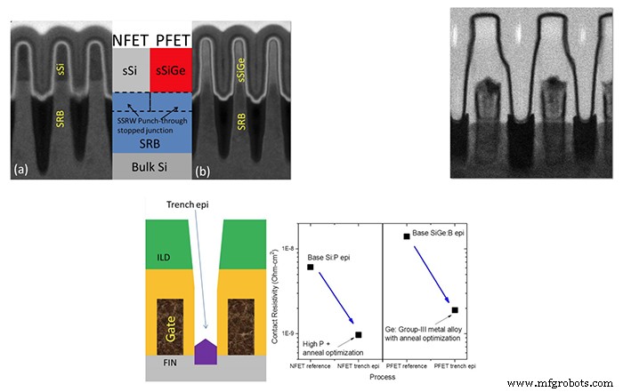
Top left: A schematic description of dual‑stressed channel materials on the SRB with a super‑steep retrograde well (SSRW), along with TEM images of (a) the tensile‑strained silicon fin and (b) the compressively strained SiGe fin on a common SRB. Top right: A TEM image of a 48 nm contacted polysilicon pitch device with an optimized self‑aligned contact with a contact opening of ~10 nm and Lmetal of ~15 nm. Bottom middle: illustration and graph show that the trench epitaxial process simultaneously meets ground rules and contact resistivity reduction following implant and anneal optimizations.
With 13.5‑nm EUV, a single, high‑fidelity exposure can produce a 7‑nm pattern, eliminating multi‑patterning. The remaining hurdle is transitioning EUV from demonstration to mass production—an evolution that parallels IBM’s System 360 legacy, which evolved into today’s advanced processors through rigorous refinement.
EUV light production begins with a molten tin droplet in vacuum, forming a spherical target. A CO₂ laser shapes and steers the droplet; a second, more powerful CO₂ laser then vaporizes the tin, emitting 13.5‑nm photons. These photons are collected and focused onto the wafer by a series of highly reflective mirrors.
Although the EUV process is complex, the team's results confirm that 7‑nm chips fabricated with EUV achieve high quality and performance. This paves the way for reliable, high‑performance components that can meet the stringent requirements of next‑generation supercomputers.
Read part one: Mapping hot spots
Read part two: Another kind of chip with carbon nanotubes
Read part three: Air spacers for 10nm chips
Nanomaterials
- 5 Key Advantages of Plastic Hinges for Modern Applications
- The Story & Science of Potato Chips: From George Crum to Modern Production
- From Nixtamal to Snack: The Complete Journey of Tortilla Chip Production
- Mastering C# Using Statements: Imports, Aliases, and Static Directives
- Advancing vs. Retarding Ignition Timing: Boosting Engine Performance Safely
- Contactless Fluid‑Level Sensing with a Reflectometer Chip
- Why Thermoset Composites Are the Smart Choice for High‑Performance Applications
- Nano‑Enhanced Concrete: Superior Strength, Faster Setting, and Lower Environmental Impact
- Mastering IPython: Boost Your Python Productivity
- Convert a Mill into a Lathe: Easy Steps for Metalworkers