


Analog Devices & Microsoft Partner to Deliver Ultra‑Accurate Time‑of‑Flight 3D Imaging
Analog Devices (ADI) and Microsoft have forged a strategic alliance to push the limits of time‑of‑flight (ToF) 3D imaging. Leveraging Microsoft’s Azure Kinect ToF platform and ADI’s world‑class IC and system integration expertise, the partnership aims to deliver solutions that are not only highly accurate but also easier to integrate across a spectrum of industries—including Industry 4.0, automotive, gaming, augmented reality, and computational photography.
Market analysts project robust growth for 3D imaging systems that can operate reliably in demanding environments. Applications such as human‑collaborative robots, room‑scale mapping, and real‑time inventory tracking are key drivers for Industry 4.0, while advanced occupancy detection and driver monitoring are essential for next‑generation automotive safety.
In a recent interview with EE Times, ADI’s Senior Director of Enhanced Imaging, Tony Zarola, and Strategic Marketing Manager Carlos Calvo outlined the foundations of this collaboration. Zarola noted, “Microsoft has set the benchmark for 3D ToF performance across image sensor manufacturers, providing ADI with the core pixel technology that underpins the sensors and solutions we’re building. Decades of expertise in data capture and revolutionary algorithms—both at the Intelligent Edge and in the Intelligent Cloud—have positioned us to combine the best of Microsoft’s and ADI’s silicon, systems, software, and optics.”
3D ToF Design Explained
Gesture recognition relies on capturing a series of human movements using a camera and IC that scans the scene in 2D or 3D. ToF technology sends a laser pulse to a target and analyzes the reflected signal, creating a depth map in real time. Unlike traditional LIDAR, 3D ToF uses high‑power optical pulses on the nanosecond scale and does not require a rotating scanner, making it ideal for short‑range, high‑resolution depth capture.
A ToF camera illuminates an object with modulated laser light and employs a wavelength‑sensitive sensor to record the reflected beam. The sensor measures the time delay between emission and reception, translating that into distance. Two common measurement methods exist: continuous‑wave (CW) and pulse. Most commercial ToF sensors use CW with CMOS technology.
Accurate ToF measurement is challenged by ambient light, multipath reflections, temperature drift, and range ambiguity. “Every component—sensor, lens, firmware—must be optimised as a cohesive system,” Calvo emphasized. “A camera with the best sensor but a poorly tuned lens will perform poorly overall.”
While RGB cameras are judged on subjective image quality, ToF cameras measure an objective physical quantity—distance. Optical imperfections such as lens flare can be benign in RGB but become performance‑critical in ToF, especially in reflective environments.
The CMOS ToF sensor integrates both emitter and receiver in a single pixel, enabling single‑pixel distance calculation at up to 160 fps. Key signal‑chain elements include the laser driver, the integrated readout sensor, and the depth‑compute engine. The design challenge spans from pixel responsivity and modulation contrast to the final 3D point‑cloud interpretation required by downstream applications.
Beyond silicon, ADI tackles the full design cycle—optomechanical layout, calibration, electrical design, and software integration—to streamline the customer experience.
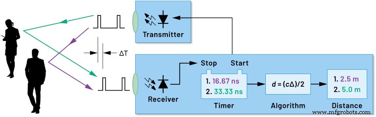
Figure 1. ToF block diagram. (source: ADI)
The sensor’s pixels capture light from distinct scene areas; their signals are combined to reconstruct the depth image. Each pixel’s operation is governed by a correlation between demodulation and modulation blocks, as illustrated in Figure 2.
The current flows to Node‑A (Da) or Node‑B (Db) during integration, governed by control signals. ClkA and ClkB run 180° out of phase during the integration period, and the phase relationship determines the DA and DB outputs. After integration, the system samples the accumulated signal (BitlineAInt1–BitlineBInt1).
Photon‑to‑electron conversion follows a Poisson distribution, and quantum efficiency—the ratio of generated electrons to incident photons—defines system performance. Ambient light adds noise, while the field of view (FoV) must be chosen to match scene coverage.
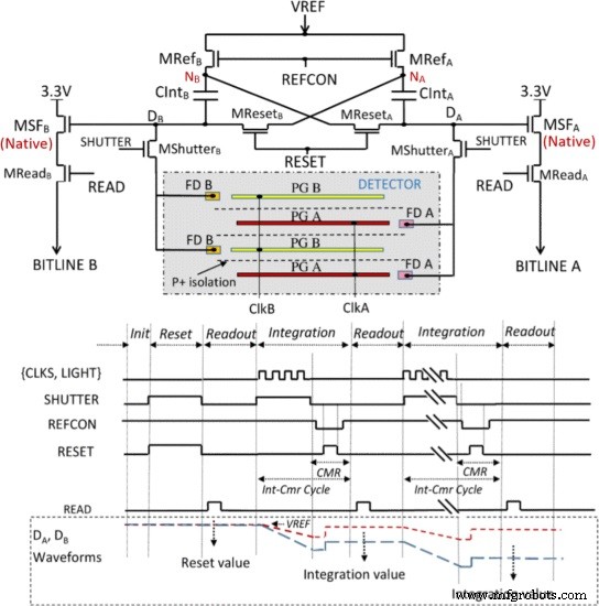
Figure 2. Electrical circuit and timing for a pixel. (Source: https://ieeexplore.ieee.org/document/6964815)
High‑frequency operation is achieved by fabricating the chip on a 0.13 µm mixed‑signal low‑power CMOS process, with minor modifications to support efficient ToF functionality.
Implications for Industry
The partnership will see ADI develop a new line of ToF 3D image sensors that deliver sub‑millimeter depth accuracy while seamlessly integrating into Microsoft’s ecosystem—leveraging Azure’s cloud capabilities and edge computing.
Zarola expressed confidence that the collaboration will transform multiple sectors: “Until now, Microsoft’s ToF technology was not widely available for commercial scaling. With ADI’s silicon and system expertise, we expect to deliver a game‑changing solution across consumer, industrial, healthcare, and automotive markets.”
Potential applications include heightened facial‑recognition security, safer factory automation, and Industry 4.0 workflows where collaborative robots can operate without safety cages. In logistics, precise ToF can automate box and pallet dimensioning, boosting efficiency.
Zarola added, “Advanced occupancy detection will improve energy use, safety systems, and human‑machine interaction. From home entertainment to automotive safety, our joint ToF platform will enable immersive gaming experiences and driver/passenger monitoring, setting the stage for tomorrow’s innovations.”
Both leaders highlighted the need for millimeter‑level depth resolution across wide temperature ranges. Achieving such precision requires 10 ps timing alignment between laser control and sensor pixels—a 1.5 mm distance error if misaligned. Additionally, maintaining accuracy across temperature variations demands sophisticated calibration algorithms developed in tandem.
Another focus is modulation frequency. “Lower modulation frequencies introduce higher depth noise and amplify multipath or ambient light artifacts,” Calvo noted. “By increasing average modulation frequency, we reduce depth noise and mitigate adverse effects.”
ADIs holistic approach—covering mechanical alignment, optical design, calibration, electrical architecture, and software—addresses the long development cycle that typically hampers ToF camera deployment.
Combining Microsoft’s ToF technology—used in HoloLens mixed‑reality devices and the Azure Kinect kit—with ADI’s custom solutions will enable a new generation of high‑performance, scalable applications, reducing time‑to‑market.
>> This article was originally published on our sister site, EE Times.
Embedded
- LTE‑M (Cat‑M1): The Future of Low‑Power 4G IoT Connectivity
- u-blox M9 GNSS Platform Achieves Meter‑Level Accuracy and Advanced Security
- Omron E3AS‑F Photoelectric Sensors Achieve 1.5‑Meter Time‑of‑Flight Detection
- MAX32520: A Secure ARM Cortex‑M4 Microcontroller Leveraging ChipDNA PUF Technology
- Bosch BMP390: 50% More Accurate Altitude Sensor for Smartphones, Wearables, and Indoor Navigation
- Memory Technologies Powering Edge AI: Challenges and Opportunities
- DUAGON-MEN-GROUP Acquires OEM Technology Solutions to Strengthen Rail Automation Expertise
- Technology’s Promise: Revolutionizing Agriculture and Food Production
- Revolutionary Data Collection Technology Boosts Speed, Accuracy, Scalability & Security at Roush Yates Engines
- How EDM Technology Drives Precise Machining: A Detailed Analysis