


Samsung Introduces I-Cube4: 4 HBMs and a Logic Die on a 100‑µm Silicon Interposer
Samsung Electronics announced the availability of its newest 2.5D packaging solution, Interposer‑Cube4 (I‑Cube4), featuring four high‑bandwidth memory (HBM) dies and a logic die on a 100 µm thick silicon interposer.
I‑Cube is a heterogeneous integration technology that places one or more logic dies (CPU, GPU, etc.) and multiple HBM dies horizontally on a silicon interposer, enabling them to function as a single chip within a single package.
I‑Cube4, developed in March as the successor to I‑Cube2, supports high‑performance computing, AI, 5G, cloud, and large‑data‑center workloads, delivering faster communication and greater power efficiency between logic and memory through heterogeneous integration.
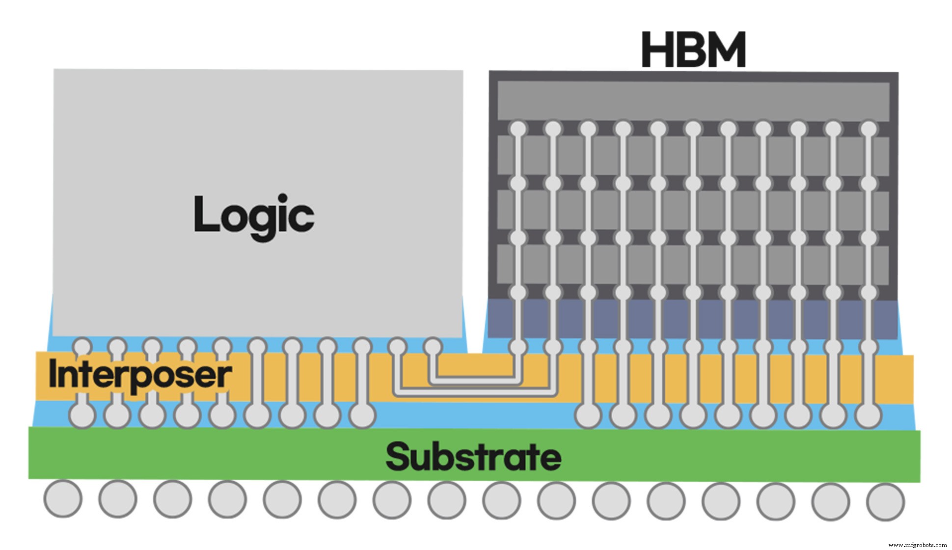
The silicon interposer area grows with the number of logic dies and HBMs. Because the I‑Cube interposer is only ~100 µm thick—thinner than a sheet of paper—larger interposers are more prone to bending or warping, which can degrade product quality. Samsung’s deep semiconductor expertise enabled rigorous studies of interposer warpage and thermal expansion, allowing adjustments to material and thickness that made I‑Cube4 commercially viable.
Samsung also introduced a mold‑free structure for I‑Cube4 that improves heat removal and yield. A pre‑screening test filters out defective products during fabrication, reducing process steps, cutting costs, and shortening lead time.
“With the explosion of high‑performance applications, it is essential to provide a total foundry solution with heterogeneous integration technology to improve the overall performance and power efficiency of chips,” said Moonsoo Kang, senior vice president of foundry market strategy at Samsung Electronics. “Leveraging the mass‑production experience from I‑Cube2 and the commercial breakthroughs of I‑Cube4, Samsung will fully support customers’ product implementations.”
Since launching I‑Cube2 in 2018 and eXtended‑Cube (X‑Cube) in 2020, Samsung’s heterogeneous integration technology has ushered in a new era for HPC. The company is now developing even more advanced packaging solutions—up to I‑Cube6 and beyond—by combining cutting‑edge process nodes, high‑speed interface IPs, and advanced 2.5D/3D packaging technologies, enabling customers to design products in the most efficient way.
Related Contents:
- Machine learning algorithm exploits ReRAM variability
- Siemens adds to Veloce for seamless hardware‑assisted verification
- Edge AI challenges memory technology
- Synopsys tackles hyper‑convergent ICs with unified circuit simulation flow
- New EDA Design Tool Addresses Heterogenous Systems Integration
Embedded
- Samsung Unveils H‑Cube 2.5D Packaging, Supporting 6‑HBM Integration for HPC & AI
- Sepro America Strengthens North American Footprint with Pittsburgh Assembly Hub and Extensive Robot Suite
- Enhanced Near‑Infrared Absorption via Two‑Step Fabrication of Structured Black Silicon and Its Device Applications
- How a Punch & Die Manufacturer Leverages IIoT for Shorter-Run, Just-In-Time Production
- Samsung Acquires Zhilabs, Enhancing 5G Innovation
- TE Connectivity Drives Digital Transformation Through Practical Manufacturing Automation
- Digital Integrated Circuits: Types & Applications
- Edm Die Sinking: Fundamentals, Techniques, and Key Benefits for Precision Metal Fabrication
- Die Casting Explained: Principles, Types, and Industrial Applications
- Choosing the Right Solar Panel for Your Product and Future Growth