


Multiband and Broadband Light Absorption in Monolayer Graphene via Magnetic Dipole Resonances in Ag Nanodisk Metamaterials
Abstract
Monolayer graphene, when suspended, absorbs only ~2.3% of incident light at normal incidence—a limitation for optoelectronic applications. We numerically demonstrate that a carefully engineered metamaterial, comprising a graphene sheet sandwiched between four silver (Ag) nanodisks of varying diameters and a SiO2 spacer on an Ag substrate, can boost graphene’s absorption to over 65% across the visible spectrum. Each nanodisk couples with the substrate to produce an individual magnetic dipole resonance; the collective action of these four resonances yields distinct absorption peaks, and by tuning their spectral overlap, a broadband high‑absorption band is realized. The absorption band can be shifted by adjusting the SiO2 thickness or the spacing between the nanodisks, offering versatile design parameters for photodetectors and related devices.
Background
Graphene’s two‑dimensional honeycomb lattice grants it exceptional electronic and optical traits, such as high carrier mobility, tunable conductivity, and remarkable transparency. Its universal absorption of ≈2.3% in the visible and near‑infrared is rooted in the fine‑structure constant, yet this value is insufficient for efficient photodetection or energy harvesting. Numerous strategies—including photonic crystal trapping, total internal reflection, surface plasmon resonance, evanescent diffraction, and guided‑mode coupling—have been explored to enhance graphene absorption. However, achieving simultaneous multiband and broadband enhancement, especially in the optical regime, remains challenging. Prior work has shown that multi‑resonator designs can broaden absorption in the THz and infrared; here we extend this concept to the visible by leveraging magnetic dipole modes in a sub‑wavelength metamaterial architecture.
Methods/Experimental
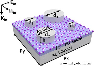
The unit cell (Fig. 1) consists of a graphene monolayer positioned between four Ag nanodisks of diameters d1 > d2 > d3 > d4 and a SiO2 spacer on an Ag substrate. Periods px and py are 400 nm, nanodisk height h is 50 nm, spacer thickness t is 30 nm, and graphene Fermi level Ef is 0.5 eV. Electromagnetic simulations were performed with EastFDTD v5.0, employing the experimental Drude‑Lorentz permittivity of Ag and a random‑phase approximation for graphene’s surface conductivity (intraband and interband terms). The graphene permittivity tensor was modeled as εg = diag(1+ iσ/(ωε0tg), 1+ iσ/(ωε0tg), 1).
Results and Discussion
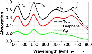
Figure 2 shows the calculated absorption spectra for graphene, Ag, and the complete metamaterial at normal incidence. Four pronounced absorption peaks appear at λ1 = 722.9 nm, λ2 = 655.7 nm, λ3 = 545.5 nm, and λ4 = 468.8 nm, with graphene absorption reaching 65.7%, 61.2%, 68.4%, and 64.5%, respectively. Compared with the intrinsic 2.3% of suspended graphene, this represents more than a 26‑fold increase. At λ3, total absorption exceeds 98.5%, mirroring the performance of established perfect absorbers and highlighting potential for solar‑cell integration.
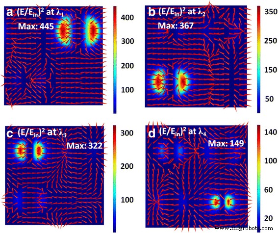
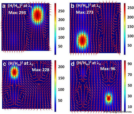
To elucidate the origins of these peaks, field distributions at each resonance were examined (Figs. 3 and 4). At λ1, electric fields localize at the edges of the largest nanodisk, while magnetic fields confine within the SiO2 spacer beneath it—characteristic of a magnetic dipole mode arising from plasmon hybridization with the substrate. Similar patterns emerge for λ2, λ3, and λ4, each associated with the next smaller disk. Thus, four independent magnetic dipole resonances drive the multiband absorption.
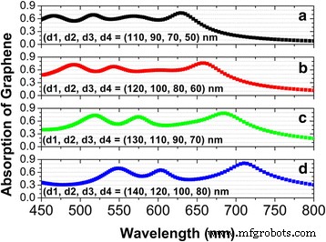
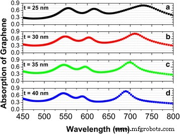
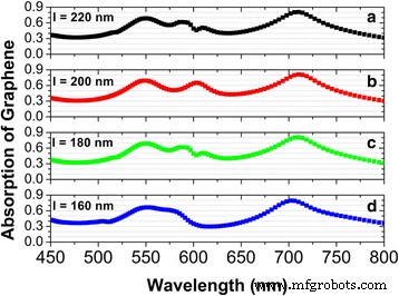
By tuning the nanodisk diameters so that the four resonances spectrally overlap, a broadband absorption band spanning 450–650 nm is achieved (Fig. 5a). Peak absorption remains above 73% while the trough stays above 50%. Gradually increasing the diameters shifts this band to longer wavelengths (Fig. 5b,c). Altering the SiO2 spacer thickness also modulates the absorption band; increasing t from 25 to 45 nm produces a clear blue‑shift (Fig. 6). Similarly, reducing the center‑to‑center distance between adjacent disks (l from 220 to 160 nm) causes a modest blue‑shift due to inter‑disk plasmon coupling (Fig. 7).
Conclusions
We have shown that a sub‑wavelength metamaterial featuring a graphene monolayer between four Ag nanodisks can generate four distinct magnetic dipole resonances, yielding multiband absorption peaks between 468 and 723 nm with efficiencies exceeding 60%. By engineering the disk diameters, spacer thickness, or inter‑disk spacing, these resonances can be merged into a broadband absorption band covering 450–650 nm with peak values above 73% and troughs above 50%. Such a tunable, high‑efficiency absorber holds promise for next‑generation photodetectors, solar cells, and other optoelectronic devices that demand strong light–matter interaction in the visible.
Nanomaterials
- Ultra‑Broadband TiN/MoS2 Metamaterial Absorber Achieves 98% Efficiency from 400–850 nm
- Coupling of Surface Plasmon Polaritons and Magnetic Dipole Resonances in Ag Nanodisk Metamaterials
- Hybrid Graphene/WO₃ and Graphene/CeOx Electrodes for High‑Performance Supercapacitors
- Alkali‑Metal‑Adsorbed Graphene‑Like GaN: Ultra‑Low Work Functions and Tunable Optoelectronic Properties
- Impact of Surface Scattering on the Absorption–Scattering Balance of Gold Nanoshells
- Angle‑Insensitive Broadband Graphene Absorber Enabled by a Multi‑Groove Metasurface
- Defect‑Driven Magnetism and Strain Engineering in Monolayer WSe2: A DFT Study
- Efficient Near‑Infrared Optical Modulation via Graphene Interband Transition Coupled to Metamaterial Magnetic Resonance
- Raman Analysis of G and D′ Phonon Shifts in Vacancy-Engineered Monolayer to Few-Layer Graphene Across 78–318 K
- From Antiferromagnetic MnBr₂ to Ferromagnetic Mn₃Br₈ Monolayer: Achieving High Curie Temperature and Large MAE