


Engineering Bandgaps in Blue Phosphorene/Graphene‑Like GaN van der Waals Heterostructures via Vertical Electric Fields
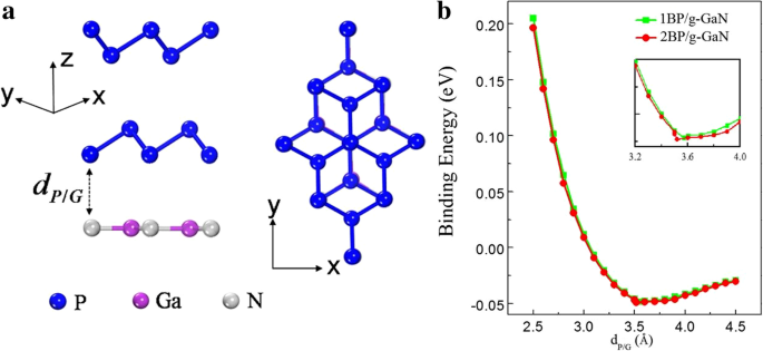
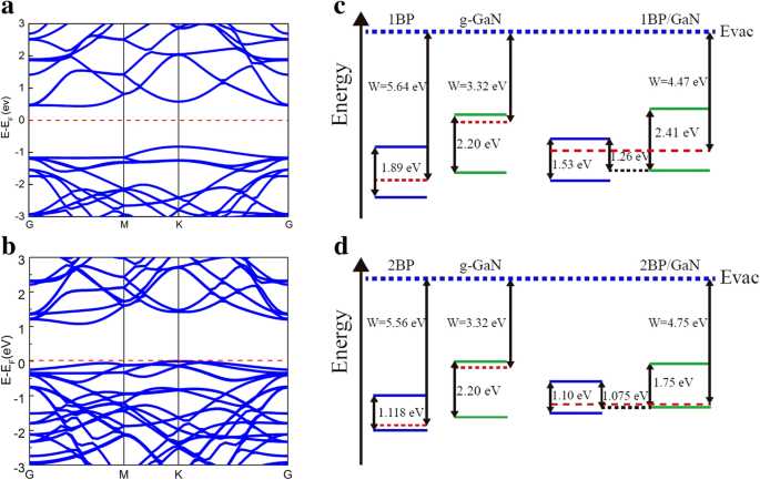
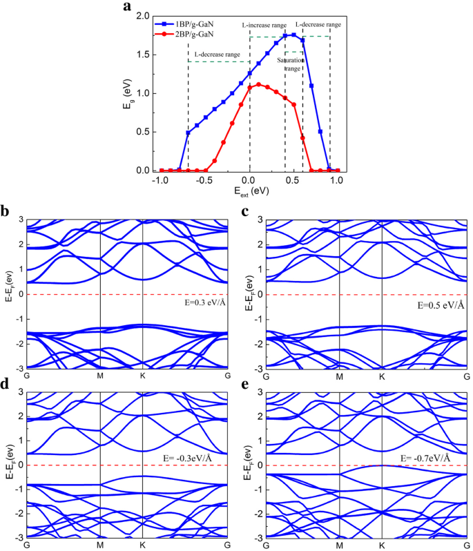
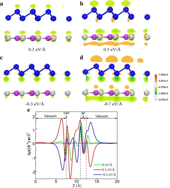
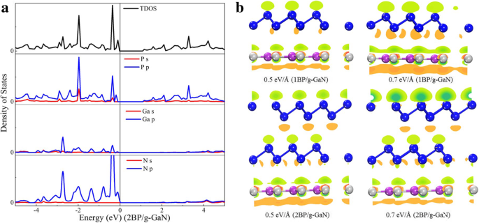
First‑principles density‑functional calculations reveal that both monolayer and bilayer blue‑phosphorene/graphene‑like GaN van der Waals (vdW) heterostructures are indirect‑gap semiconductors with a type‑II band alignment. The bandgap (Eg) can be tuned linearly by an external vertical electric field (Eext), displaying a pronounced Stark effect. When the field exceeds a critical value (≈0.9 eV/Å for the monolayer and ≈0.7 eV/Å for the bilayer), the heterostructure undergoes a semiconductor‑to‑metal transition. Two‑dimensional (2D) materials—graphene, transition‑metal dichalcogenides, black phosphorene, and the recently reported graphene‑like GaN (g‑GaN)—continue to attract attention because of their remarkable electronic and optical properties and their potential for next‑generation nanoelectronic devices. Blue phosphorene (blue‑P), a corrugated monolayer of phosphorus, has been epitaxially grown on Au(111) and GaN(001) substrates, and it offers a sizable bandgap and high carrier mobility. g‑GaN, synthesized by migration‑enhanced encapsulated growth, is an indirect‑gap semiconductor that can be efficiently modulated by an external electric field. The close lattice match (~2 %) between blue‑P and g‑GaN makes the blue‑P/g‑GaN vdW heterostructure an attractive platform for engineering band structures and exploring interlayer charge transfer. Despite intensive studies on blue‑P/TMDs and blue‑P/graphene heterostructures, little is known about the electronic behavior of blue‑P/g‑GaN systems. Here we employ vdW‑corrected DFT to investigate the band structure, band alignment, and field‑induced bandgap modulation of monolayer and bilayer blue‑P/g‑GaN heterostructures. The CASTEP package was used to perform plane‑wave DFT calculations with a projector‑augmented‑wave (PAW) basis. Exchange‑correlation effects were treated with the generalized gradient approximation (PBE), and the bandgap was refined using the HSE06 hybrid functional. van der Waals interactions were included via Grimme’s DFT‑D2 scheme. A 500 eV plane‑wave cutoff and a 7 × 7 × 1 k‑point mesh were adopted for geometry optimization; electronic states were sampled with a 21 × 21 × 1 grid. A vacuum layer of 20 Å along the c‑axis ensured negligible interaction between periodic images. Structural relaxations were performed until forces dropped below 0.001 eV/Å. Optimized lattice constants of monolayer blue‑P and g‑GaN are 3.25 Å and 3.20 Å, respectively, yielding a lattice mismatch of only ~2 %. The equilibrium interlayer spacing is 3.57 Å for the monolayer and 3.52 Å for the bilayer, with binding energies of ≈49 meV—comparable to other vdW systems such as BP/graphene. Band‑structure calculations show indirect gaps of 1.26 eV (GGA) and 2.20 eV (HSE06) for the monolayer heterostructure, and 1.075 eV (GGA) / 1.91 eV (HSE06) for the bilayer. The conduction‑band minimum lies near the M point while the valence‑band maximum is at K, confirming a type‑II (staggered) alignment. The work‑function difference between the composite and pristine blue‑P is ΔEF = –1.17 eV for the monolayer and –0.81 eV for the bilayer, consistent with the observed band offsets. Applying a vertical external field (Eext) modulates Eg following a Stark‑like linear dependence. For the monolayer, Eg increases with positive fields up to 0.5 eV/Å, then saturates and finally decreases when the field exceeds 0.6 eV/Å, eventually closing the gap at ≈0.9 eV/Å. The bilayer exhibits a similar trend but reaches the semiconductor‑to‑metal transition at a lower field (≈0.7 eV/Å). Negative fields cause a linear reduction of Eg, with the gap vanishing near –0.8 eV/Å for the monolayer and –0.5 eV/Å for the bilayer. Charge‑density analyses reveal that the electric field drives electrons from the blue‑P layer to the g‑GaN layer under positive bias, and the reverse under negative bias. The accumulated charge is strongest at ±0.5 eV/Å, confirming the field‑induced charge transfer that underpins the Stark effect. Projected density‑of‑states calculations indicate that the valence‑band maximum is dominated by g‑GaN states, while the conduction‑band minimum derives primarily from blue‑P, reinforcing the type‑II alignment. First‑principles calculations demonstrate that monolayer and bilayer blue‑P/g‑GaN vdW heterostructures are indirect‑gap semiconductors with type‑II band alignment. The bandgap can be tuned linearly by a vertical electric field, exhibiting a pronounced Stark effect, and the structures undergo a controllable semiconductor‑to‑metal transition when the field exceeds ≈0.9 eV/Å (monolayer) or ≈0.7 eV/Å (bilayer). These findings provide a clear pathway for designing electrically tunable 2D optoelectronic devices based on blue‑P/g‑GaN heterostructures.Abstract
Introduction
Computational Methods
Results and Discussion
Conclusion
Abbreviations
Nanomaterials
- Tuning Electronic and Optical Anisotropy in Monolayer GaS via Vertical Electric Fields
- Structural, Electronic, and Magnetic Characterization of Ag<sub>n</sub>V (n = 1–12) Clusters via DFT and CALYPSO Search
- Electric Field Control of Non‑Volatile Magnetism in Co₂FeAl / PMN‑PT Heterostructures at Room Temperature
- Tunable Electronic Properties of Bilayer α‑GeTe under Variable Interlayer Spacing and External Electric Fields
- Fast Reverse Recovery in Ge‑Doped Vertical GaN Schottky Barrier Diodes
- V, Cr, Mn Edge‑Functionalized Armchair Phosphorene Nanoribbons: Half‑Semiconductors and Spin‑p‑n Diodes
- Enhanced Baliga’s Figure‑of‑Merits in a Novel GaN Nano‑Pillar Vertical FET with 2DEG Channel and Patterned Substrate
- Band‑gap Engineering in InGaNBi Quaternary Alloys: Composition‑Dependent Structural, Electronic, and Strain Properties
- How Interlayer Coupling and Van Hove Singularities Shape MoS₂ Multilayer Electronics and Optics
- Tuning Schottky Barriers and Contact Types in Graphene–MoTe₂ van der Waals Heterostructures via Strain and Electric Fields