


Graphene Nanoribbons: Precision Fabrication and Emerging Electronics Applications
Graphene’s Unique Electronic Landscape
Pure graphene is a zero‑band‑gap semiconductor; its valence and conduction bands meet, which is ideal for continuous electronic conduction but problematic when an on/off switch is required. By narrowing graphene into ribbons only a few nanometers wide, a band gap can be induced. For instance, dense arrays of 10 nm‑wide ribbons exhibit a band gap of approximately 0.2 eV, opening the door to transistor‑grade performance.
Advanced Production Techniques
Unlike conventional top‑down lithography, modern approaches build graphene nanoribbons (GNRs) atom‑by‑atom from small‑molecule precursors, ensuring uniform width and edge structure. Key fabrication routes include:
- Graphite nanotomy – A diamond knife slices bulk graphite into nanoblocks that are then exfoliated into GNRs (Berry group).
- Unzipping carbon nanotubes – Multi‑walled tubes are opened in solution with potassium permanganate and sulfuric acid (Tour group), or via plasma etching when partially embedded in polymer films.
- Bottom‑up growth on SiC – Ion implantation followed by vacuum or laser annealing yields GNRs directly on silicon carbide substrates.
Bottom‑up methods produce ribbons with near‑identical dimensions and atomically smooth edges, essential for high‑mobility electronic transport.
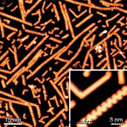
Record‑Low‑Width Ribbons
Researchers at IBM and the University of California, Riverside have fabricated the thinnest GNR arrays yet—each ribbon only 10 nm wide—on silicon‑carbide wafers. Achieving such narrow widths with conventional lithography alone is nearly impossible, but a hybrid process combining e‑beam (or standard photolithography) with block‑copolymer self‑assembly (using PS/PMMA lamellae) enables mass production. These arrays cover roughly 50 % of the device channel, delivering the high current densities needed for integrated circuits.
Through meticulous control of ribbon width, edge termination, and array density, these GNRs promise exceptional electronic performance, bringing graphene closer to mainstream nanoelectronic applications.
Nanomaterials
- Graphene Enables Precise Nanomaterial Placement for Industrial‑Scale Device Integration
- Graphene‑Based Loudspeakers and Earphones: Ultra‑Low‑Power, High‑Fidelity Sound
- High‑Efficiency Graphene Solar Cells: 9% Power Conversion with TFSA Doping
- Hybrid Graphene/WO₃ and Graphene/CeOx Electrodes for High‑Performance Supercapacitors
- Infrared Electromagnetic Field Redistribution on Graphene by Silver Nanoparticle Dimers
- Secondary Transfer of Graphene Electrodes for Highly Stable Flexible OLEDs
- Ultra‑Smooth Copper Substrates Enhance Graphene Quality: Annealing + Electro‑Polishing
- Predicting Surface Impedance of Metasurface–Graphene Hybrid Structures in the Terahertz Regime
- Controlled Low‑Temperature Growth of WSe₂ on Graphene for Efficient p‑Type Transistors
- Dynamic Control of Photodetector Responsivity in Graphene Nanoribbon Devices