Industrial manufacturing
Nanomaterials

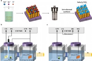
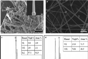
AbstractTiO2 is an attractive semiconductor suitable for photocathodic protection, but its weak absorption of visible light and low quantum yield limit its usage. Here, a new heterostructured SnIn4S8 nanosheet/TiO2 nanotube photoanode was prepared and its photocathodic protection performance was ana
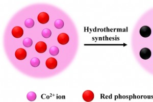
AbstractIn this work, cobalt phosphide nanoparticles (Co2P NPs) were prepared by simple and mild hydrothermal method without the use of harmful phosphorous source. The morphological structure and surface component of Co2P were characterized by transmission electron microscopy, X-ray diffraction and
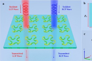
AbstractIn this paper, we present a plasmonic chiral metasurface absorber (CMSA), which can achieve high selective absorption for right-handed and left-handed circular polarization (RCP, “+”, and LCP, “−”) lights at optical frequency. The CMSA is composed of a dielectric substrate sandwiched with b
AbstractA simple fabrication of end-bonded contacts InAsSb NW (nanowire) array detector to weak light is demonstrated in this study. The detector is fabricated using InAsSb NW array grown by molecular beam epitaxy on GaAs substrate. The metal-induced gap states are induced by the end-bonded contact
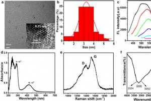
AbstractIn recent years, multifunctional nanoparticles with combined diagnostic and therapeutic functions show great promise in nanomedicine. In this study, we report the environmentally friendly synthesis of fluorescent carbon nano-dots such as carbon quantum dots (CQDs) by microplasma using o-phen
AbstractGaAs nanostructures have attracted more and more attention due to its excellent properties such as increasing photon absorption. The fabrication process on GaAs substrate was rarely reported, and most of the preparation processes are complex. Here, we report a black GaAs fabrication process

AbstractOver the last couple of decades, the advancement in Microelectromechanical System (MEMS) devices is highly demanded for integrating the economically miniaturized sensors with fabricating technology. A sensor is a system that detects and responds to multiple physical inputs and converting the
AbstractCu2SnS3, as a modified material for high-capacity tin-based anodes, has great potential for lithium-ion battery applications. The solvothermal method is simple, convenient, cost-effective, and easy to scale up, and has thus been widely used for the preparation of nanocrystals. In this work,
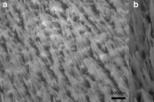
AbstractPeriodically ordered arrays of vertically aligned Si nanowires (Si NWs) are successfully fabricated with controllable diameters and lengths. Their photoconductive properties are investigated by photoconductive atomic force microscopy (PCAFM) on individual nanowires. The results show that the
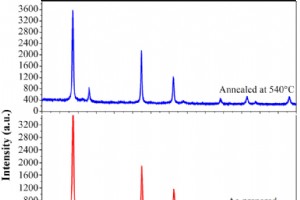
AbstractHigh-quality Sn(IV)-doped CdS nanowires were synthesized by a thermal evaporation route. Both XRD and Raman scattering spectrum confirmed the doping effect. The room temperature photoluminescence (PL) demonstrated that both near bandgap emission and discrete trapped-state emission appeared s
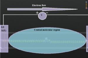
AbstractDoping is the key feature in semiconductor device fabrication. Many strategies have been discovered for controlling doping in the area of semiconductor physics during the past few decades. Electrical doping is a promising strategy that is used for effective tuning of the charge populations,

AbstractHere we report the ZrOx-based negative capacitance (NC) FETs with 45.06 mV/decade subthreshold swing (SS) under ± 1 V VGS range, which can achieve new opportunities in future voltage-scalable NCFET applications. The ferroelectric-like behavior of the Ge/ZrOx/TaN capacitors is proposed to be
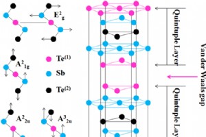
AbstractDiscovery of two-dimensional (2D) topological insulators (TIs) demonstrates tremendous potential in the field of thermoelectric since the last decade. Here, we have synthesized 2D TI, Sb2Te3 of various thicknesses in the range 65–400 nm using mechanical exfoliation and studied temperature co
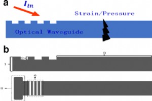
AbstractBased on the related characteristics of optical waveguide and flexible optical materials, a flexible and stretchable optical waveguide structure oriented to tactile perception is proposed. The sensing principle of optical waveguide is based on mechanical deformation caused by output light lo
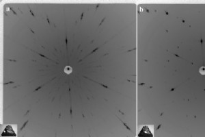
AbstractThe detailed studies of the surface structure of synthetic boron-doped diamond single crystals using both conventional X-ray and synchrotron nano- and microbeam diffraction, as well as atomic force microscopy and micro-Raman spectroscopy, were carried out to clarify the recently discovered f
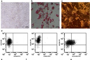
AbstractExosomes derived from human umbilical cord mesenchymal stem cells (hucMSCs) expressing microRNAs have been highlighted in human diseases. However, the detailed molecular mechanism of hucMSCs-derived exosomal miR-18b-3p on preeclampsia (PE) remains further investigation. We aimed to investiga

AbstractResearches pivoting on histone deacetylases (HDACs) in depression have been excessively conducted, but not much on HDAC1. Therein, the present study is launched to disclose the mechanism of HDAC1/microRNA (miR)-124-5p/neuropeptide Y (NPY) axis in depression. Sprague Dawley rats were stimulat
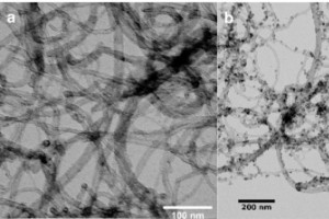
AbstractCarbon-based materials are the spearhead of research in multiple fields of nanotechnology. Moreover, their role as stationary phase in chromatography is gaining relevance. We investigate a material consisting of multiwall carbon nanotubes (CNTs) and superparamagnetic iron oxide nanoparticles
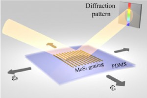
AbstractIn this paper, we report a new type of MoS2-based grating sensor for in-plane biaxial strain gauges with a precision limit of ~ 1‰. The MoS2 grating is numerically simulated with different biaxial strains up to 5%. Our first-principles calculations reveal that the strain sensitivity of the M
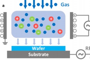
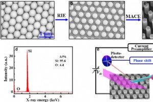
AbstractWe analyzed the dry etching of perovskite oxides using argon-based inductively coupled plasmas (ICP) for photonics applications. Various chamber conditions and their effects on etching rates have been demonstrated based on Z-cut lithium niobate (LN). The measured results are predictable and
Nanomaterials