Industrial manufacturing
Nanomaterials

Last year the world consumed almost 97 million barrels of oil per day. Yet, a significant portion of that reserve remains trapped within the same wells—up to 60 % of a reservoir’s oil can be locked in capillaries only tens to hundreds of nanometers wide (for context, DNA is 2.5 nm across). The porou
Carbon nanotubes (CNTs) are attractive to the semiconductor sector because they deliver exceptional electrical conductivity while being only 1 nm thick—far thinner than silicon. Despite this promise, CNT‑based chips are absent from mainstream devices. The roadblocks remain large‑scale integration a
Nanotechnology refers to the manipulation of matter at the scale of a few nanometers (nm). For context, a sheet of paper is roughly 100,000 nm thick. By mastering the unique phenomena that emerge at this scale, scientists can develop devices that are smaller, faster, and more energy‑efficient. At

Gerber and Binnig reflect on the invention of the AFM. Last week, IBM’s Zurich Research Lab celebrated two major recognitions that underscore its pivotal role in advancing nanoscience. The first honor came from the Kavli Foundation and the Norwegian Academy of Science and Letters, which organized a

National Inventors’ Day honors the brilliance of inventors worldwide. At IBM Research Zurich, we sat down with Master Inventor Lukas Czornomaz to discuss his career and the patents that define his impact. Lukas Czornomaz and Veeresh Deshpande take home the Best Student Paper Award of the IEEE 2016
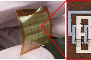
For the last few decades, the relentless scaling of transistors on rigid silicon wafers has driven unprecedented gains in performance for personal gadgets and high‑end computing. Yet emerging fields such as real‑time edge analytics and the Internet of Things demand high‑performance logic and sensor

After 30 years and more than 9,000 citations, the inventors of the Atomic Force Microscope (AFM) have been awarded the Kavli Prize in Nanoscience. Gerd Binnig and Christoph Gerber in the 1990s. The Kavli Prize is shared between Gerd Binnig, Christoph Gerber and Calvin Quate. Binnig and Gerber were
Today, the World Economic Forum’s Meta-Council on Emerging Technologies released its 2016 Top 10 Emerging Technologies list, spotlighting innovations poised to enhance lives, transform industries, and protect the planet. “Horizon scanning for emerging technologies is crucial to staying abreast of d
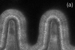
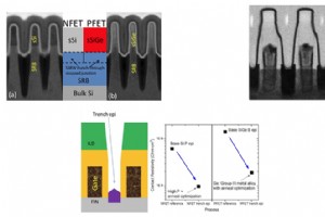
At IBM Research in Albany, NY, our semiconductor team is pushing CMOS technology toward 10 nm, 7 nm, and future nodes. As device dimensions shrink, transistor channel resistance becomes a decisive factor in chip performance. Innovating the channel material to lower that resistance is therefore es
The ultra‑high‑vacuum electron microscope tucked away in a lab on the ground floor of the IBM Thomas J. Watson Research Center in Westchester County, NY, is a powerful tool for uncovering the physics that govern materials at the nanoscale. By visualizing how structures behave under extreme condition
Envision a future where routine annual check‑ups are complemented by a cost‑effective home diagnostic chip. By analyzing a single urine sample, patients can continuously monitor their baseline health, and any subtle biomarker shift—potential early cancer signals or viral infection—can be detected p

Manuel Le Gallo’s research will inspire a new generation of extremely dense neuromorphic computing systems. (Source: IBM Research – Zurich) Drawing inspiration from the human brain’s spike‑based communication, IBM Research in Zurich has engineered artificial neurons that emulate the “integrate‑an

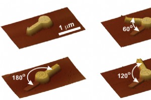
Earlier this year, researchers from ETH Zurich and IBM Research – Zurich unveiled a groundbreaking technique for constructing artificial molecules from 1‑µm microspheres, published in Science Advances. These minute particles, roughly the size of bacteria, hold promise for future micro‑robots, photon

IBM Research scientist Qing Cao unveils a breakthrough method to interconnect carbon nanotubes. The impending slowdown of silicon‑based chips has long prompted researchers to seek alternatives. IBM’s Qing Cao claims carbon nanotubes (CNTs) – cylindrical sheets of carbon only a few atoms wide – offe
This is the third of a four‑part series on IBM’s cutting‑edge papers presented at IEDM 2016. The International Electron Devices Meeting is widely regarded as the world’s premier forum for breakthrough research in semiconductor and electronic device technology, design, manufacturing, physics, and mod
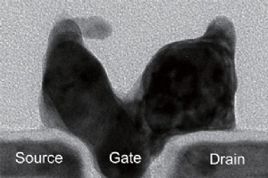
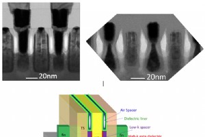
This fourth installment of our four‑part series explores IBM’s groundbreaking papers presented at IEDM 2016. IEDM, the world’s leading forum for semiconductor and electronic device innovation, hosted IBM’s latest breakthroughs: a scanning‑probe thermometer, an air spacer for 10‑nm chips, a 7‑nm Fin
Early detection dramatically improves outcomes. For instance, breast and prostate cancers diagnosed at stage I achieve almost 100 % five‑year survival, whereas stage IV rates drop to 26 % and 28 %, respectively. Despite this, many patients seek care only after symptoms appear, by which time the dise
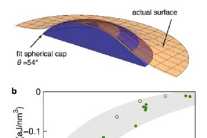
The IBM laboratory that pioneered the scanning tunneling microscope (STM) and atomic force microscope (AFM) has introduced a new, indispensable tool for nanoscale research: a scanning probe thermometer capable of measuring temperatures with millikelvin precision. Accurately gauging the temperature o
Dr. Griselda Bonilla serves as Senior Manager of IBM Research’s Advanced BEOL Interconnect Technology team, steering breakthroughs that elevate the company’s industry‑leading on‑chip interconnect (BEOL) solutions. We spoke with her prior to her team’s presentations at the IITC/AMC Conference in San
Nanomaterials