


IBM Breaks New Ground: First Liquid‑Phase Atomic Imaging of 2D Materials at Room Temperature
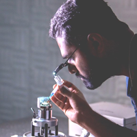
Peter Nirmalraj investigates the properties of 2D layered materials using a C60 functionalized metal STM probe in the noise‑free labs at the Binnig and Rohrer Nano‑technology Center. (Source: Marcel Begert, IBM Research–Zurich)
Over 35 years after Nobel laureates Gerd Binnig and Heinrich Rohrer invented the scanning tunneling microscope, IBM scientists in Zurich have achieved another milestone in atom‑by‑atom imaging—this time in liquid environments.
In partnership with researchers from the University of Limerick, École Polytechnique Fédérale de Lausanne, and the University of Massachusetts–Amherst, IBM team members Peter Nirmalraj, Bernd Gotsmann, and Heike Riel engineered and demonstrated a robust molecular STM probe that operates at room temperature in liquid, enabling the analysis of emerging two‑dimensional layered materials.
This represents the first successful use of a molecular STM probe with Ångstrom‑scale resolution in a liquid medium under standard laboratory conditions, a feat previously limited to ultrahigh‑vacuum (UHV) or cryogenic environments.
The findings are detailed in the paper “A robust molecular probe for Ångstrom‑scale analytics in liquids,” published today in Nature Communications.
I spoke with Peter, a specialist in molecular surface science and liquid‑phase scanning probe microscopy, to learn more about this breakthrough.
Which element of the probe’s design enabled the high resolution you achieved in your paper?
Peter Nirmalraj: We transitioned from a non‑functionalized gold STM probe to chemically terminating the tip with a single C60 molecule. This reduces apex reactivity and enriches the spatial information obtainable from the material. Achieving such atomic‑level control in liquid at room temperature was a significant challenge.
What is particular to imaging under standard laboratory conditions, as opposed to the common UHV and cryogenic conditions?
PN: The core difficulty lies in maintaining the stability of the single molecule at the tip apex. Picture an inverted mountain capped with a cherry—this scale captures the sensitivity required. While cryogenic conditions suppress fluctuations, at room temperature the molecule remains energetically and dynamically active, leading to instability. Our work demonstrates that a delicate probe can be stabilized in high‑density liquids that dampen the motion of the anchored molecule.
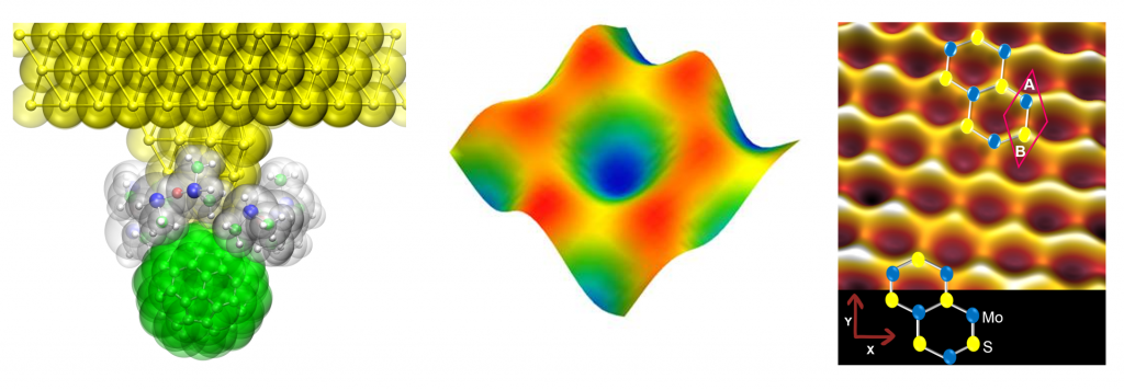
From left to right: Fullerene‑terminated gold STM probe; a single‑atomic hexagon of monolayer graphene highlighting carbon lattice sites; atomic structure of 2D molybdenum disulfide with selectively analyzable species.
When the World Economic Forum named 2D materials one of the top 10 emerging technologies of 2016, the ability to probe them at atomic resolution in realistic environments became increasingly critical. Accurate knowledge of their ambient compatibility, environmental robustness, and electronic properties is essential for manufacturers of thin‑film transistors, transparent, and flexible electronics.
“Our technique allows faster and more reliable structural and electronic fingerprinting of a rapidly growing body of 2D materials.”
—Peter Nirmalraj, IBM Research scientist
By combining the highest achievable resolution with experimentally challenging conditions, we unlock valuable information that directly informs 2D material‑based device engineering.
What steps must be taken next to advance imaging at liquid–solid interfaces?
PN: The next milestone is to resolve single molecular elements with sub‑molecular resolution. Experimentally and theoretically, we must deepen our understanding of the coupling mechanisms between the tip‑anchored molecule and the surrounding liquid, and assess how the molecule’s electronic and structural influence enhances spatial contrast.
About the author: Millian Gehrer is a summer intern at IBM Research – Zurich, where he interviews scientists to learn about their work and motivations. In the fall, he will begin studying Computer Science as an undergraduate at Princeton University.
Nanomaterials
- Inside Vayyar’s 4D Imaging Radar SoC: Design, Applications, and Market Impact
- IBM Scientists Measure Thermal Conductance of Single-Atom Gold Contacts at Room Temperature
- Revolutionizing Quantum Computing: Single‑Atom Qubits Controlled by Scanning Tunneling Microscopy
- Scientists Successfully Synthesize and Visualize Cyclo[18]Carbon
- Atomic‑Resolution Imaging of Molecular Charge States
- Visualizing Oceanic Dissolved Carbon at the Atomic Scale
- Nanotechnology: From In‑Vivo Imaging Systems to Controlled Drug Delivery
- Pseudospin‑Controlled Unidirectional Transmission in Graphene Topological Plasmonic Crystals
- Dual‑Mode MRI/Fluorescence Nanoprobe cRGD‑Gd‑Cy5.5 for Targeted Imaging of Integrin αvβ3‑Positive Tumors
- Magic Mathematical Relationships Governing Nanocluster Geometry and Properties