


CNT Breakthroughs in Transistor Scaling and Integration Pave the Way for Next‑Gen Chips
Carbon nanotubes (CNTs) are attractive to the semiconductor sector because they deliver exceptional electrical conductivity while being only 1 nm thick—far thinner than silicon. Despite this promise, CNT‑based chips are absent from mainstream devices. The roadblocks remain large‑scale integration and transistor scalability. Recent papers we co‑authored in Science and Nature Nanotechnology present promising solutions to both challenges.
Footprint achievement tips the nanoscale
Scaling is the first hurdle. Three‑dimensional FinFET silicon devices are approaching their power and performance ceiling at a 7 nm gate length. Even the latest 5 nm silicon nanosheet transistors, while delivering higher density and speed, will eventually reach their own limits.
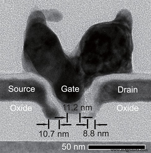
A transistor is more than its gate. The Source, Drain, and spacers all add up for a total footprint. Pictured: a CNT transistor with a 40nm footprint. (Figure 1B in “Carbon nanotube transistors scaled to a 40‑nanometer footprint”, published in Science.)
In our Science paper, “Carbon nanotube transistors scaled to a 40‑nanometer footprint,” we demonstrated a complete CNT transistor that meets the ITRS target of a 40 nm footprint—a benchmark unchanged since 2015. By comparison, the most advanced commercial 14 nm devices occupy roughly 90 nm of chip area.
The intrinsic 1.2 nm thickness of CNTs allows for gate lengths as short as 10 nm, delivering superior electrostatic control and reduced leakage. Moreover, carrier mobility in CNTs surpasses that of silicon, boosting overall device speed.
However, integrating CNTs with their source and drain required a novel contact strategy. Earlier end‑bonded contacts demanded processing temperatures near 850 °C, prohibiting channel lengths below 60–100 nm. By replacing the wiring material with a cobalt‑molybdenum alloy, we reduced the thermal budget to 650 °C, enabling 10 nm channel spacings.
Lead author Dr. Qing Cao and colleagues confirmed that, within this 40 nm footprint, CNT transistors meet or exceed the performance metrics of contemporary silicon devices.
CNT elements come together on ring oscillator
Showing that a single, highly scaled transistor is feasible—despite a non‑ideal process—has driven our pursuit of comprehensive CNT integration. Over the past five years, we have refined techniques for sorting semiconducting CNTs, guiding their self‑assembly across wafers, and producing robust n‑channel CNT field‑effect transistors that resist degradation from metal oxidation.
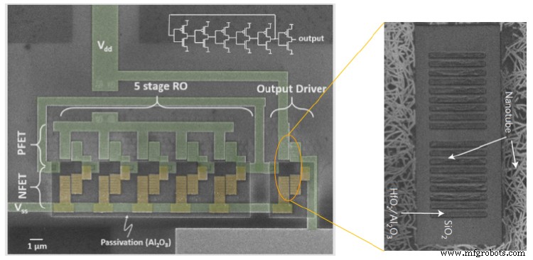
All elements have to work simultaneously in a functional ring oscillator. Pictured: Top‑view scanning electron microscopy image of a 5‑stage CNT ring oscillator and CNTs placed trenches. (Figure 1B in “High‑speed logic integrated circuits with solution processed self‑assembled carbon nanotubes”, published in Nature Nanotechnology.)
In early‑stage disruptive technologies, solutions for one problem can inadvertently compromise other device or circuit components. This trade‑off has historically constrained nanotechnology demonstrations—including CNTs—to low integration levels, raising concerns about their practical viability.
Our Nature Nanotechnology paper, “High‑speed logic integrated circuits with solution‑processed self‑assembled carbon nanotubes,” demonstrates a breakthrough: assembling all necessary components into a fully functional CMOS ring oscillator, a widely used benchmark for logic technologies.
Dr. Jianshi Tang and collaborators merged our established purification and placement techniques—visualized as isolated ‘penne‑pasta’ CNTs in solution—with a pivotal addition: a sidewall oxide that shields the n‑FET channel throughout fabrication. This modification tripled the yield, ensuring that every element of the ring oscillator operates reliably.
The 5‑stage CMOS ring oscillator described—operating at the industry‑standard 1 V—achieves a stage‑switching frequency of 2.8 GHz (355 ps) despite a modest CNT density (only six CNTs visible in the channel). This marks the first nanotechnology demonstration to surpass the 1 GHz threshold. Extrapolating to a CNT density exceeding 100 CNTs µm⁻¹ with appropriately scaled devices, we project sub‑picosecond stage delays, far outpacing current silicon technology.
As we write in the paper:
Since CMOS ring oscillators directly reflect the maturity of the technology, it is long‑awaited proof that the important issues of transitioning this promising material into a real technology are being vigorously resolved.
Nanomaterials
- Carbon Nanotubes Deliver Record Flexibility and Speed in Electronics
- Carbon Nanotube Yarns, Artificial Muscles, and Transparent Sheets: Advanced Applications
- Heating‑Enhanced Dielectrophoresis Yields Ultrahigh‑Density, Aligned Single‑Walled Carbon Nanotube Films
- Optimizing Carbon Nanotube Materials and Composites through Advanced Porosimetric Characterization
- High‑Performance Na4Mn9O18/Carbon Nanotube Cathodes for Aqueous Sodium‑Ion Batteries
- Electrochemical Energy Storage: Enhancing Capacitance with Reduced Graphene Oxide/Carbon Nanotube Composites
- Optimizing Vertically Aligned Carbon Nanotube Growth: The Key Role of Oxide Buffer Layers in CVD
- Ethanol‑Driven Direct CVD Growth of High‑Quality Graphene on SiO₂ via an Intermediate Carbon Nanotube Stage
- Advances in Carbon Nanotube Assembly and Integration for Next‑Generation Applications
- NASA-Developed MEMS Accelerometer & Gyroscope Using High-Strength Carbon Nanotube Tape