


IBM Zurich Lab Earns Dual Honors: Kavli Laureates Symposium & EPS Historic Site Designation
Gerber and Binnig reflect on the invention of the AFM.
Last week, IBM’s Zurich Research Lab celebrated two major recognitions that underscore its pivotal role in advancing nanoscience.
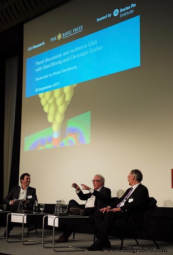
The first honor came from the Kavli Foundation and the Norwegian Academy of Science and Letters, which organized a public symposium featuring 2016 Kavli Laureates in Nanoscience, Gerd Binnig and Christoph Gerber. The event, held at the SwissRe Center for Global Dialogue in Rueschlikon, Switzerland, drew nearly 200 guests, including diplomats, state secretaries, Nobel laureate K. Alex Müller, and about 50 students from Norwegian and Swiss universities.
During the symposium, the laureates discussed their groundbreaking work—Binnig and Gerber were awarded the Kavli Prize “for the invention and realization of atomic force microscopy (AFM), a breakthrough in measurement technology and nanosculpting that continues to have a transformative impact on nanoscience and technology.” A highlight was a panel discussion where the audience asked, “How do you know when you are on the right path to a eureka moment?” Binnig answered poetically: “My strategy is, I prove to myself that this is the wrong path, and if I can’t prove this is the wrong path, I continue.” (Watch a replay of the entire event: Video 1, Video 2)
Just as the symposium concluded, IBM’s Zurich Lab received its second accolade: the European Physical Society (EPS) named the site a Historic Site. The announcement, made during a ceremony attended by the Mayor of Rueschlikon and Nobel laureate K. Alex Müller, highlighted the lab’s legacy as the first industrial laboratory on the EPS Historic Sites List, alongside iconic locations such as Einstein House Bern and the CERN Synchrocyclotron.
Dr. Rüdiger Voss, EPS President, remarked, “This IBM location has achieved many firsts, including the first industrial lab on the EPS Historic Sites List. This will hopefully encourage industry to keep investing in basic research as the foundation for scientific progress.”
?Proud day for us in Zurich – the IBM lab was just named a historic site by the @EuroPhysSoc joining @CERN and Einstein House Bern pic.twitter.com/NEbHKyjB7q
— IBM Research (@IBMResearch) September 26, 2017
Nanomaterials
- IBM Engineers Develop Nanoscopic Thermometer, Enabling Precise Temperature Mapping of Quantum Devices
- IBM Research Team Wins 2017 Innovation Award for Pioneering InGaAs/SiGe CMOS Technology
- IBM Showcases Seven Breakthroughs for Chips Beyond 7nm at SPIE
- IBM and Warwick Scientists Capture First High‑Resolution Image of Triangulene, a Highly Reactive Triangular Molecule
- IBM Researchers Demonstrate Groundbreaking Rocking Brownian Motors for Precise Nanoparticle Separation
- Last Chance to Register for PT Tech Days – Expert Sessions on Injection Molding & Extrusion
- Top Metal Finishing Techniques: Choose the Best Method for Superior Surfaces
- Optimizing Cutting Fluids for Different Metal Cutting Processes
- Comprehensive Guide to Lathe Cutting Tools: Types, Applications, and Selection Tips
- Effective Techniques to Dry Compressed Air for Reliable Equipment Performance