


IBM Showcases Seven Breakthroughs for Chips Beyond 7nm at SPIE
When IBM first unveiled functional 7 nm test chips in 2015 in partnership with GLOBALFOUNDRIES and Samsung, we anticipated rapid manufacturing readiness within a year. Today, the semiconductor industry is accelerating, and IBM is charting the path to the next generation of nodes beyond 7 nm.
At this year’s International Society for Optics and Photonics (SPIE) Advanced Lithography conference, IBM presented seven papers that illuminate the technological advances driving the transition beyond the 7 nm node, all centered on Extreme Ultraviolet (EUV) lithography.
Achieving sub‑nanometer transistor dimensions and atomic‑scale interconnects demands patterning techniques that are both high‑resolution and process‑efficient. EUV offers a single‑exposure solution that surpasses the resolution limits of earlier lithography methods. The seven SPIE presentations highlight critical developments in EUV mask design, resist chemistry, and process integration—cornerstones for reliable 7 nm and future nodes.
Design Intent Optimization for Beyond‑7 nm Nodes
Michael Crouse, Nicole Saulnier, and Derren Dunn demonstrate that modest adjustments to wiring geometry can dramatically improve EUV printability. Figure 1 shows how optimized mask shapes enable continuous, unbroken lines at dimensions below the 7 nm threshold, reducing electrical variability and enhancing yield.
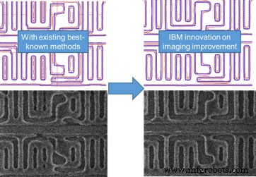
Figure 1: Contrast optimization on 2‑D metal wiring. With this improvement, features 20–30 % smaller than those achieved in the 7 nm node can be robustly printed, significantly lowering physical and electrical variability.
Exploring Novel EUV Mask Stacks
Martin Burkhardt’s simulations cover the entire periodic table to identify mask materials that can deliver higher contrast without requiring changes to EUV optics. Fabricating masks from these advanced alloys could enable seamless scaling beyond 7 nm while maintaining current EUV infrastructure.
Quantifying Line‑Edge and Line‑Width Roughness
Ravi Bonam presents a comprehensive methodology for measuring and minimizing roughness in EUV‑printed lines. His work pinpoints process conditions that yield the smoothest features, directly improving manufacturability and chip performance.
Enhancing Resist‑Hardmask Interfaces
Dario Goldfarb investigates the chemistry between EUV resists and inorganic hardmasks. By tailoring surface interactions—illustrated in Figure 2—he achieved the first reliable patterning of resists on silicon hardmasks, a critical step for transferring EUV patterns into the substrate.
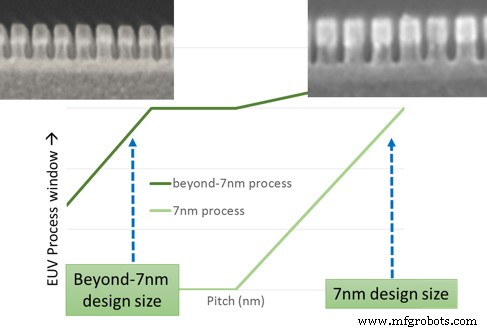
Figure 2: An EUV resist previously incompatible with an inorganic silicon hardmask is now successfully patterned after surface customization.
Polymer Brush Adhesion Layers
Indira Seshadri shows that a thin polymer brush can serve as an adhesion promoter between EUV‑printed features and the substrate. This approach preserves design fidelity during etching, ensuring high yield at the smallest feature sizes.
Reducing Defect Density in Composite EUV Films
Luciana Meli presents a systematic defect‑inspection workflow that identifies material and process improvements necessary for the low defectivity required at 7 nm and beyond.
Single‑Expose Patterning for Sub‑30 nm Features
Anuja De Silva demonstrates single‑exposure EUV patterning of wiring circuits at 30 nm and smaller—dimensions that push beyond the 7 nm node. Figure 3 illustrates the leap from the first 7 nm capabilities to the next generation, highlighting both the progress and remaining challenges.
Figure 3: Integrated imaging and materials innovations enable IBM to produce the feature sizes required beyond the 7 nm node.
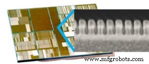
A 7 nm chip packs 20 billion transistors onto an area the size of a fingernail, enabling unprecedented performance in data analytics, cognitive computing, and the next wave of mobile applications. The research presented at SPIE propels the industry toward robust, single‑exposure EUV processes and paves the way for continued scaling and performance gains.
Additional IBM Presentations at 2017 SPIE
- Design intent optimization at the beyond 7 nm node: The intersection of DTCO and EUVL stochastic mitigation techniques – Michael Crouse, Nicole Saulnier, Derren Dunn
- Investigation of alternate mask stacks in EUV lithography – Martin Burkhardt
- Decomposition of the TCC using non‑coherent kernels for faster calculation of lithographic images – Alan Rosenbluth
- Development of Ti‑containing hardmasks through PEALD deposition – Anuja De Silva
- DSA patterning options for logics and memory applications – Charlie Liu
- Electrical study of DSA shrink process and CD rectification effect at sub‑60 nm using EUV test vehicle – Cheng Chi
- Reaching for the True Overlay in Advanced Nodes – Chiew‑Seng Koay
- Topcoat‑free Strategies for Orientation Control of All‑organic High‑χ Block Copolymers – Dan Sanders
- Identification and reliability sensitivity analysis of a correlated ground rule system (design arc) – Eric Eastman
- Advanced fast 3D DSA model development and calibration for design technology co‑optimization – Kafai Lai
- Unexpected Impacts of RIE Gases onto Lithographic Films – Martin Glodde
- Electrical Test Prediction using Hybrid Metrology and Machine Learning – Mary Breton
- Reducing LER in Si and SiN Through RIE Optimization for Photonic Waveguide Applications – Nathan Marchack
- Directed Self‑Assembly Patterning Strategies for Phase Change Memory Applications – R. Bruce
- Materials characterization for process integration of multi‑channel gate all‑around (GAA) devices – Raja Muthinti
- Comprehensive analysis of line‑edge and line‑width roughness for EUV lithography – Ravi Bonam
Nanomaterials
- High‑Performance Tungsten‑Titanium Alloy Targets for Advanced Semiconductor Chips
- Ultra‑High‑Purity Tungsten Targets: Key to Advanced Semiconductor Thin Films
- IBM Engineers Develop Nanoscopic Thermometer, Enabling Precise Temperature Mapping of Quantum Devices
- IBM's Air Spacer Innovation Paves Way for 10 nm FinFET Chips
- Silicon‑Germanium FinFETs: Pioneering Low‑Resistance Channels for 7nm and Beyond
- IBM Zurich Lab Earns Dual Honors: Kavli Laureates Symposium & EPS Historic Site Designation
- IBM Research Team Wins 2017 Innovation Award for Pioneering InGaAs/SiGe CMOS Technology
- IBM Researchers Demonstrate Groundbreaking Rocking Brownian Motors for Precise Nanoparticle Separation
- 7 Essential Principles for Peak Machining Performance
- Essential BGA Chip Layout Tips for Optimal Performance